Quick and Accurate Measurement of Lead Lifting in Semiconductor Packages
With growth in automobile communication and electronic control, and demand for smaller and thinner sized devices such as smartphones, tablets, and wearable devices, requirements for higher mounting quality and reliability are increasing. Particular attention is required for the pins of semiconductor packages (lead frame packages) because lifting of the pins can result in connection failures and reduced connection strength.
This section explains basic knowledge of lead frames and lead lifting, problems in conventional measurement of lead lifting, and the latest measurement method that not only solves these problems but also dramatically improves work efficiency and accuracy.
- Lead Frames (Leads)
- Lead Frame Materials, Processing, and Applications
- Lead Lifting, Connection Failures, and Other Surface Mounting Problems
- Problems in Conventional Measurement of Lead Lifting
- Solution to Problems in Lead Lifting Measurement
- Summary
Lead Frames (Leads)
A lead frame is a component that supports and fixes a semiconductor chip (semiconductor element) in a semiconductor package such as an integrated circuit (IC) or large scale integrated (LSI) circuit. It connects to external wiring by means of outer leads, which are multiple external connector terminals that project from a package like the legs of a centipede.
A finished semiconductor package of this type is called a lead frame package, and the outer leads projecting from the resin are simply called leads. The following figures show the name of each part in a lead frame and the internal structure of a semiconductor package.
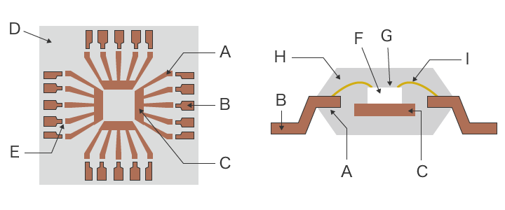
- A
- Inner lead
- B
- Outer lead
- C
- Die pad
- D
- Frame
- E
- Dam bar
- F
- Semiconductor chip (semiconductor element)
- G
- Electrode pad
- H
- Resin package
- I
- Bonding wire
Lead Frame Materials, Processing, and Applications
Lead frames are ordinarily made from thin sheets of copper (Cu) alloy, iron (Fe) alloy, or similar material with excellent properties including electrical conductivity, mechanical strength, thermal conductivity, and corrosion resistance.
Progressive precision pressing (punching, drawing, and bending) is performed using a long strip of this thin sheet. A series of processes forms the die pads which support and fix semiconductor chips (semiconductor elements), inner leads (which connect to the semiconductor elements), outer leads (which connect to external wiring), and other necessary parts. In addition to machining processes, the lead frame manufacturing process also includes etching, plating, and other surface treatment processes.
Lead frames are not only used in packages for IC and LSI circuits, but also for discrete semiconductors, photocouplers, LEDs, and other components. In all of the components above, wire bonding is used to connect semiconductor element electrodes and the inner leads.
Lead Lifting, Connection Failures, and Other Surface Mounting Problems
In recent years, with increasingly smaller sizes of mounted electronic devices and increased density of electronic circuits, a higher level of accuracy is required for lead frames and their connections. In the surface mounting process, defects in the dimensions and shapes of outer leads and coplanarity defects can result in problems during mounting. Lead lifting of surface mount devices (SMDs) may occur as a result of various factors including insufficient spread (low wettability) of solder paste caused by improper lead surface treatment or insufficient reflow heating, insufficient solder melting caused by inappropriate reflow conditions, and PCB warpage. This lifting can result in connection failures and reduced connection strength.
The following are possible causes of lead lifting and other typical mounting defects, and examples of countermeasures to them.
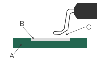
Lead lifting (incorrect part seating)
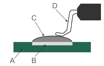
- A
- PCB
- B
- Mounting pad
- C
- Solder
- D
- Lead (part) lifting
- Problem: Outer leads and other electronic part terminals remain unsoldered and become lifted.
- Causes: Misalignment of solder paste printing or parts, uneven amount of printed solder paste, uneven melting time, deformation of leads or other terminals, and insufficient mounter pressure
- Countermeasures: Correct the positions, reduce the flux content, inspect and control the shapes of leads and other terminals and review the printing and reflow conditions.
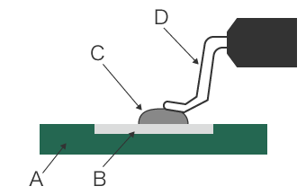
Insufficient melting of solder
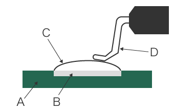
- A
- PCB
- B
- Mounting pad
- C
- Remaining solder powder
- D
- Lead lifting
- Problem: Solder does not fully melt and solder powder remains. This results in problems such as reduced connection strength of mounted components and lifting of leads.
- Causes: Inappropriate reflow conditions, deteriorated solder paste
- Countermeasures: Review the reflow conditions, and check or change the solder paste storage method.
No soldering
- A
- PCB
- B
- Mounting pad
- C
- Insufficient or missing solder (lead connection failure)
- Problem: There is no solder on the mounting pad or the amount of solder is extremely small.
- Causes: Insufficient amount of printed solder paste, insufficient wettability caused by the surface conditions of the mounting pads and leads or by deteriorated solder paste, and insufficient reflow heating
- Countermeasures: Check the conditions of the mounting pad and lead surfaces, printing masks, and solder paste. Review the reflow conditions.
Insufficient spread of solder paste
- A
- PCB
- B
- Mounting pad
- C
- Solder (insufficient spread)
- D
- Lead
- Problem: The solder does not spread sufficiently onto the mounting pads and leads, resulting in reduced connection strength and lead lifting.
- Causes: Insufficient amount of printed solder paste, deteriorated mounting pads, leads, or solder paste, or insufficient reflow heating
- Countermeasures: Check the conditions of the mounting pad and lead surfaces, printing masks, and solder paste. Review the reflow conditions.
Uneven amount of solder
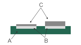
- A
- PCB
- B
- Mounting pad
- C
- Solder (uneven amount or height)
- Problem: The amount of solder at soldered parts is not constant. This causes lead lifting and connection failures.
- Causes: Low printability (suitability for screen printing) of solder paste or incorrect printing conditions
- Countermeasure: Review the solder paste and printing conditions.
Problems in Conventional Measurement of Lead Lifting
It is not easy to check the connection conditions for the numerous leads that are present on a single mounted semiconductor package. Measurement to check the conditions becomes even more difficult for smaller electronic parts and components and for PCBs where the mounting density is higher.
Measurement using a conventional height gauge or coordinate measuring machine (CMM) involves the following problems.
Problems in measurement of lead lifting using a height gauge
A height gauge can be used in combination with a dial gauge to measure height.
Because only points can be measured, it is necessary to spend much time and measure a large number of points in order to improve accuracy. However, even when much time is invested and many points are measured, it is still impossible to identify the conditions of the entire surface.
For the leads of semiconductor devices that are densely mounted on a PCB, it may be difficult to perform contact measurement at extremely small parts in narrow sections. Variation in measurement results between different operators and error in the measuring instrument also make stable measurement impossible.
Problems in measurement of lead lifting using a coordinate measuring machine
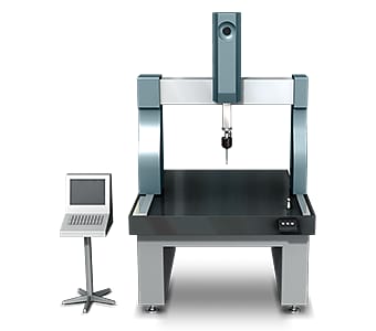
When measuring using a coordinate measuring machine, it is necessary to contact multiple points on the measurement target surface with the probe tip.
However, even slight bending of the PCB or components caused by the measurement pressure of the probe can produce variation in the measured values.
Additionally, as the locations of leads in a semiconductor package are small, it is necessary to prepare a precision program for the measuring machine in advance. Some leads cannot even be measured due to the connection size or position.
Solution to Problems in Lead Lifting Measurement
The contact-type measuring instruments that are ordinarily used require much time to perform measurement because they measure three-dimensional targets and areas by means of point contact. There are also the problems of low measurement value reliability due to variation caused by human factors and the difficulty in creating usable data from the numbers and other post-processing.
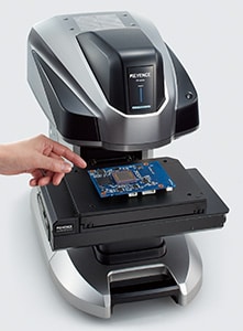
To resolve these measurement problems, KEYENCE has developed the VR Series 3D Optical Profilometer.
The VR Series accurately captures the 3D shape of the entire target surface without contacting the target. A 3D scan of the target on the stage can be completed in as little as one second for high accuracy measurement of the 3D shape. It is capable of instantaneous and quantitative measurement with no errors in the measurement results. This section introduces some specific advantages of the VR Series.
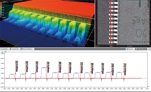
Advantage 1: Complete measurement in as little as one second. The 3D shape of the entire target surface can be captured accurately with a single measurement.
The VR Series acquires area data (at 800,000 points in one scan) in as little as one second, dramatically reducing the time required for measuring large numbers of points. It allows accurate measurement and quick evaluation of the 3D shape across the entire target.
Differences in multiple lead heights can be visualized in a color map making it possible to identify at a glance which leads are lifted and how much lifting has occurred. Once a scan is completed, profile measurement of any part can be performed at a later time allowing the detailed conditions to be identified.


Advantage 2: Able to easily perform quantitative measurement of small targets.
By switching between the low magnification and high magnification cameras, accurate 3D scanning of the entire shape or detailed parts can be performed even for small targets such as the leads of semiconductor devices.
3D shape measurement can be performed easily just by placing the target on the stage and pressing a button. Because automatic position adjustment is possible based on target feature data, strict positioning is not required. This makes quantitative measurement possible without variation caused by human factors regardless of the level of operator experience and knowledge; this makes it possible to increase the number of samples that can be measured within a given time.
For setup, this series includes the industry’s first Smart Measurement function that automatically configures the measurement range and moves the stage. This eliminates the work required to set the measurement length, Z-range, and other settings.
Summary
The VR Series can accurately and instantaneously measure the 3D shape of the entire surface by high-speed, non-contact 3D scanning to identify lead lifting, the mounting conditions of each part, and other necessary items.
- Measurement can be completed in as little as one second. Lifting (heights) of multiple leads can be captured as a surface can be identified in the color map. Detailed data can be acquired by performing profile measurement of the desired cross-section.
- By switching the magnification, it is possible to measure the entire shape or detailed parts of small and delicate mounted components with high accuracy and by non-contact means.
- No positioning is required. No experience or knowledge is required. Just place the target on the stage and press a button to complete measurement.
- The 3D shape can be displayed in a color map. Being able to share data that is visually easy to understand allows smooth coordination and countermeasures to be carried out.
- Multiple sets of measurement data can be easily and quantitatively compared and analyzed.
This makes it possible to perform side-by-side comparisons of multiple sets of measurement data. Analysis can be performed by applying settings to all data sets at once. By sharing the 3D shape data acquired using the VR Series, it is possible to dramatically reduce the required time and improve the efficiency of the entire process including measurement, defect analysis, and defect countermeasures.
