Instantaneously and Accurately Measuring Solder Fillet Shapes
The use of telecommunication and electronic controllers in automobiles is continuing to grow. As a result of increasing miniaturization and densification of devices such as smartphones, tablets, smart watches and other wearable devices, mounting quality of these devices and quality assurance are becoming increasingly advanced and important.
This page explains basic knowledge of the solder fillets and mounting processes that are closely related to PCB mounting quality. It also introduces countermeasures to fillet shape defects and mounting defects, problems in shape measurement and evaluation, and a solution to these problems.
- Solder Fillets
- Surface Mount Technology (SMT) Process, Solder Fillet Shape, Mounting Defects and Countermeasures
- Problems in Conventional Solder Fillet Shape Measurement
- Solution to Problems in Solder Fillet Shape Measurement
- Summary
Solder Fillets
A solder fillet in PCB mounting refers to the part where solder is applied around the components that are mounted on a PCB. Soldering quality is evaluated based on the solder fillet shape.
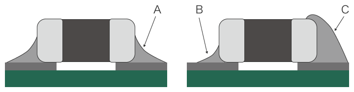
Good solder fillet shape
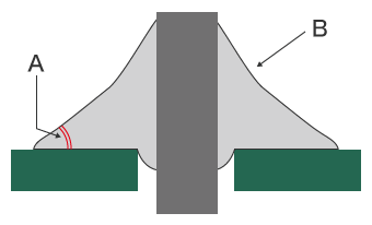
- A
- Angle: 15° to 45°
- B
- Smooth curved concave shape with luster (A convex shape is called a solder blob and may cause mounting defects.)
It is important to check and evaluate the melted and solidified solder shape (fillet) at the part which connects to the land. The shape should be a smooth concave curve like the slopes of Mount Fuji. As explained in the figure below, a smaller contact angle θ (higher wettability) indicates better conditions.
However, when heating is insufficient or there is too much solder, it solidifies in a convex shape like a water droplet. This is called a solder blob, and it may cause a reduction in bond strength or a connection defect.
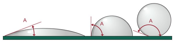
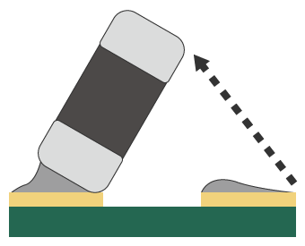
Contact angle θ and wettability
Wettability is expressed as the value of contact angle θ between the solid object surface and the liquid (such as melted solder) that was dripped on it. A smaller angle A in the figure (contact angle θ) means higher wettability, and indicates that the liquid was properly applied to the solid object surface. A larger angle means lower wettability because the solid object surface has repelled the liquid.
Surface Mount Technology (SMT) Process, Solder Fillet Shape, Mounting Defects and Countermeasures
This section explains the general process of surface mount technology (SMT), amount of solder used for surface mounting, fillet shape, and mounting defects.
Example of a surface mount technology (SMT) process
General processes of surface mount technology (SMT) for FA (Factory Automation) are listed below.
- • Solder paste (cream solder) printing process
- Using a high precision metal mask (plate or screen mask), cream solder (solder paste) is applied by screen-printing with a squeegee so the paste is applied only to the necessary locations on the PCB. In prototyping or small quantity production, an inkjet printer that requires no mask may be used.
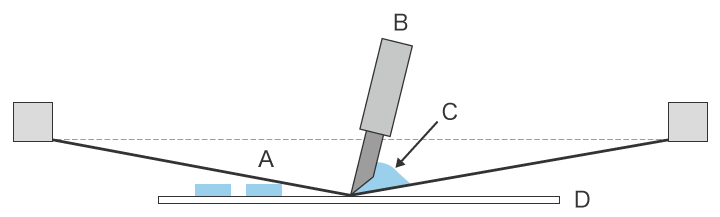
- A
- Metal mask
- B
- Squeegee
- C
- Solder paste (cream solder)
- D
- PCB
- • Chip bonding process
- This process applies bond for mounting chip components onto the PCB. It is primarily used in the flow solder process to fix the components in place so they do not fall off when mounting components. The use of electroconductive adhesives, make it possible to fix the components in place and also achieve continuity.
- • Chip mounting process
- The cassette which contains the mounting components wound in a reel is installed on the mounter. The mounter automatically places the mounting components in the specified positions on the supplied PCB according to the program.
- • Reflow process
- After solder paste or chip bond is applied and the mounting components are placed in position, the PCB is transported into the reflow oven and heated. This heating melts the solder paste so that it wets and spreads out on the mounted components and PCB mount pad. It then cools and solidifies to complete soldering. At the same time, this heating also cures the chip bond in order to fix the bonded components in place.
- Because the solder melting temperature and chip bond curing temperature are different, the heating temperature and cooling speed must be adjusted within the process. Caution is required in the reflow process due to the risk of PCB warpage caused by heat.
Solder fillet shape, mounting defects and countermeasures
For the solder fillet, a suitable amount of solder must be applied in a shape that covers the component terminal electrode and mount pad.
For example, when mounting a commonly used multi-layer chip capacitor, when the amount of solder is correct, the fillet forms inward gently curving slope lines on the right and the left terminal electrodes. When too much solder is applied, it forms a solder blob as explained before. When the amount of solder is too little, it is not possible to create a fillet with sufficient shape and volume. In both cases, bond strength is reduced and mounting defects or connection defects may occur.
- A
- Correct solder amount and fillet shape (Conditions must be the same at both electrodes.)
- B
- Insufficient amount of solder and fillet shape defect
- C
- Excessive amount of solder and fillet shape defect
During the reflow process, surface tension is produced by the melted solder at the terminal electrodes. When there is a difference between the amounts of solder on the two terminals or variation in the heating temperature, a difference in the surface tension occurs at the two terminals and causes the problem known as the “Manhattan phenomenon.” The name comes from the fact that the standing chip resembles a tall building. It is also referred to as the “tombstone phenomenon” for looking similar to a tombstone.
When formulating defect countermeasures, in addition to solder amount and quality, it is important to consider the process conditions including preheating of the reflow oven and optimizing the temperature rise profile.
Consideration is also required at the preceding stage of PCB design for factors such as the land shape and heat countermeasures that will allow a correct fillet to form easily. In some cases, improving the metal mask used when printing the solder paste (cream solder) may help to improve soldering accuracy.
Problems in Conventional Solder Fillet Shape Measurement
Below, we explain the problems with fillet measurement and evaluation using conventional profile measurement systems.
Problems in solder fillet shape measurement using contact-type profiling systems
A profile measurement system measures and records the profile of a target by tracing its surface with a stylus.
Positioning and leveling as well as other preparation of the target is vital to measurement performance requiring a specialized operator to perform advance setup and measurement work. This requires much time and labor.
Since measurement of a fillet that has a 3D shape is performed using lines, it is not possible to identify the entire shape, and measurement of small-size and high-density PCB may be difficult.
Solution to Problems in Solder Fillet Shape Measurement
So far, we have explained the solder fillet shape using 2-dimensional figures, however the actual fillet has a 3-dimensional shape. A variety of fillet shape defects can occur in insertion mounting and surface mounting.
For this reason, when measuring the fillet shape and inspecting its appearance, an accurate evaluation of the fillet is only possible with precision measurement tool that can measure the 3D shape (including the surface area, height, volume, and inclination). Because conventional measurement tools are limited to measuring lines, it is difficult to accurately identify the fillet shape.
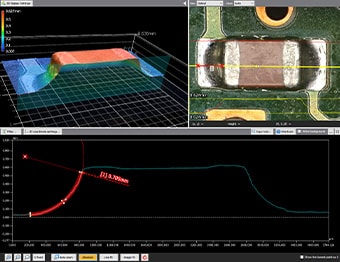
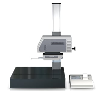
To resolve these measurement problems, KEYENCE has developed the VR Series 3D Optical Profilometer. This tool accurately captures the 3D shape of the entire target surface without contacting the target.
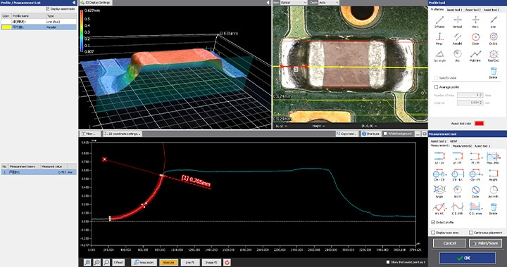
With this system, positioning of a target is not required. Users can take accurate and repeatable measurements in as little as 1 second by simply by placing the sample on the stage and clicking a single button. This makes it possible to accurately measure 3D profiles and 2D cross-sectional shapes and allows any type of user to quickly and easily perform quantitative measurement and evaluation without variation in the measurement results. This section introduces some specific advantages of the VR Series.
Advantage 1: 3D shape of an entire surface can be captured in as little as 1 second.
Because a fillet gauge measures the shape fitting conditions on a line, and a profile measurement system measures the fillet surface by stylus contact on a line, it is difficult to accurately measure the entire fillet shape.
With the VR Series, user can scan the 3D surface shape of the target in order to instantaneously complete non-contact measurement in as little as one second.
Because it is possible to switch between low magnification and high magnification, high-accuracy measurement can be performed not only of the entire mounting PCB but also of the detailed solder fillet shape at specific components.
Its height color map, makes it possible to visualize the shape of the fillet or electronic component, allowing abnormal locations and their detailed values to be quickly identified.
Once a part is scanned, the measurement data is stored and profile measurement of the cross-section on any line can be performed at any time using past data. This data can be easily shared, making it possible to smoothly perform tasks such as identifying the cause of a defect, formulating countermeasures to prevent defect recurrence, and carrying out comparisons and trend analysis.

Advantage 2: Fillet shapes can be measured instantaneously without advance setup or positioning.
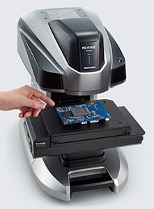
The VR Series allows measurement to be started right away without fastening the target to a jig, performing strict positioning, or any other difficult advance setup or operation of the measurement system.
3D shape measurement can be performed easily just by placing the target on the stage and pressing a button. Because automatic position adjustment is possible based on the target characteristic data, strict positioning is not required. This makes quantitative measurement possible without variation caused by human factors. Any user, regardless of experience level can take accurate and repeatable measurements increasing the number of samples that can be measured in a given time.
Additionally, this series includes the industry’s first Smart Measurement function that automatically configures the measurement range and moves the stage. This eliminates the work required to set the measurement length, Z-range, and other advanced settings.
Summary
In addition to solder fillet shapes, the VR Series can instantly and accurately measure the full 3D surface of an object allowing users to visualize mounting conditions on the entire PCB by non-contact, high-speed 3D scanning.
- Measurement can be completed in as little as one second. The solder fillet (height) of a surface can be identified in the color map, and detailed data can be acquired by profile measurement of the desired cross-section.
- By switching the magnification, it is possible to measure the entire shape or detailed parts of small and delicate mounted components with high accuracy and by non-contact means.
- No positioning is required. No experience or knowledge is required. Just place the target on the stage and press a button to complete measurement.
- The target can be represented however needed using combinations of the 3D shape color map image, target image, and profile data. Being able to share data that is visually easy to understand allows smooth coordination and countermeasures at each process.
- A larger number of samples can be measured in a short time. Quantitative comparison and analysis of multiple sets of measurement data can be performed easily.
This makes it possible to perform side-by-side comparisons of multiple sets of measurement data, and to perform data analysis by applying settings to all data sets at once. By sharing 3D shape data acquired using the VR Series, it is possible to dramatically reduce the required time and improve the efficiency of the entire process from measurement, defect analysis, and defect countermeasure.
