Screen Printing
Overview of screen printing
Screen printing is a generic term for printing with systems that use a plate (screen mask) made of a screen mesh woven with synthetic fiber such as polyester or metal fiber such as stainless steel. As a type of stencil printing, screen printing involves passing ink through the fine mesh of a screen mask by the pressure of a squeegee or other tool in order to print (coat) the ink onto the target (substrate).
- Basic principle of screen printing
-
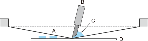
- A. Plate (screen mask)
- B. Squeegee
- C. Ink
- D. Target (substrate)
Screen printing can be used for many kinds of materials—so many that it is sometimes said the method can print on "everything except for water and air." These systems are used for printing on various objects seen in daily life, including T-shirts and other clothes (textiles); cups, glasses, and dishes (ceramics and glass); and automotive instruments, electronics, and electric appliances (resins and metals).
In recent years, the technologies incorporated in making the plates, printers, and inks have advanced to enable printing of extremely fine lines. Today, the majority of applications involve state-of-the-art electronics field that require ultra-fine coating with a high aspect ratio.

Present state of screen printing
Pioneering "printed electronics" technology
Against a backdrop of the recent trend toward smaller and lighter-weight electronics and electric appliances, and the low price competition in the global market, "printed electronics" using high-resolution screen printing has garnered greater as a technology for effective production of precision electronic circuits and devices.
Among the various coating systems such as gravure coaters and inkjet coaters, selecting screen printing for high-resolution pattern coating, such as wiring on electronic components, enables the following advantages:
- Screen printing can be used with almost any type of substrate
- Screen printing can be used even with substrates featuring uneven or round surfaces
- High flexibility in design and selection of coating material ingredients, including paste ink
- Advanced technology that supports high-resolution patterns (Example: Line widths of 15 to 30 μm)
- Thick film formation for printing wiring with a high aspect ratio
High-resolution pattern printing (coating) is currently done either with screen printing that requires a plate (screen mask), or inkjet printing that performs patterning directly from data without the need to make a plate. The selected method depends on the properties of the substrate and ink, production lot, takt, and so on.
- Example of multiple printing (coating) in PCB manufacturing
-
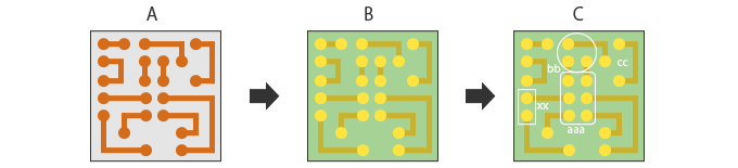
- Conductive paste coating: Wiring patterns are formed by printing.
- Resist coating: All areas other than the points to be connected are masked for protection.
- Character printing: Parts symbols or other characters are printed.
Applications of screen printing
In recent years, printed electronics technology has been faced with an increase in the following demands:
- Thin film coating for thinner electronic devices with higher density internal structures
- Thick film coating for improving circuit insulation
- Coating of highly viscous material in ultrafine lines
- Improved printing (coating) position accuracy for supporting miniaturization of electronic devices
Screen printing has evolved and developed as a means of satisfying these demands, specifically used in the following applications.
- Multi-layer ceramic capacitors (MLCCs)
- Electrode layers are printed as thin as possible in multiple layers to achieve miniaturization and larger capacity.
- Multi-layer inductors (chip coils)
- Coil patterns are printed in multiple layers with conductive ink on ferrite or dielectric ceramic sheets. High-resolution printing enables chip miniaturization.
- Chip resistors
- Terminal electrodes and resistive elements are printed on thin ceramic PCBs through screen printing. After printing, a laser cuts the resistive element while the resistance of each chip is measured to obtain the target resistance.
- Cream solder printing
- A paste of cream solder (solder powder and flux) is applied on a PCB, and components are mounted automatically. The PCB is then sent through a reflow furnace to achieve precision soldering.
- Touch panel sensors
- Screen printing and photolithography can be used for making transparent electrode patterns on touch panels. The former has the advantage of higher production efficiency and lower costs, while the latter has the advantage of high-resolution patterning.
- Flexible devices (FPCs)
- Printing is possible on flexible PCBs (FPCs) made of PET films. Screen printing can be used not only for patterning but also for thick coating, hole plugging, and layer stacking. Highly efficient manufacturing of 3D products such as PE products and sensors is also possible.
- MEMS (Micro Electro Mechanical Systems)
- Becoming increasingly popular in recent years, flexible MEMS uses screen printing to form an ultra-precision coil structure by coating high viscoelastic conductive paste on plastic PCBs.


