Semiconductor Wafer and Glass Substrates Inspection
In the manufacturing processes of semiconductor wafers—which requires high accuracy—or of glass substrates—the essential component of an LCD—the uniform layer thickness of adhesive and resist will have a direct effect on product quality. This section introduces coating inspection improvement and adoption examples, as well as useful cases for improving equipment operation and processes requiring high accuracy.

- Column: Inline 100% inspection of wafer outer diameters
- Column: Confirmation of wafer setting height inside equipment
- Gap measurement for slit coaters
- Column: Positioning of glass substrates
Column: Inline 100% inspection of wafer outer diameters
In semiconductor manufacturing, as many chips as possible are laid out on a wafer to increase chip production. However, if the outer diameter of a wafer is slightly smaller than the specification, the chips positioned along the circumference of the wafer will be defective. In such cases, the wafer cannot yield the designed number of acceptable chips, resulting in lower production.
Conventional offline sample inspection does not eliminate out-of-specification wafers from the process.
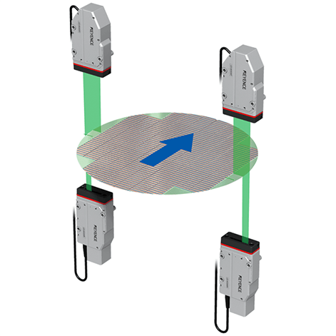
The introduction of the High-speed Optical Micrometer LS-9000 Series enables inline 100% wafer diameter inspection before processing.
For example, passing a wafer between the LS-9000 Series transmitter and receiver during transferring to the processing equipment enables outer diameter measurements in the order of microns.
With a high-speed measurement processing of 16,000 cycles per second, measurement will not affect the takt time. Instantaneous detection of deviation or inclination of the target during transfer is also possible, allowing for automatic correction before measurement. This ensures stable measurement in the line under various conditions.
Column: Confirmation of wafer setting height inside equipment
In mass-production of semiconductors, even subtle inclination or height differences between wafers set in the processing equipment will cause defective processing. The accuracy required for equipment operation is extremely high. To maintain processing quality, measurement and monitoring absolutely must be conducted inside the equipment.
With conventional non-contact measurement systems, however, installing the units in the small space inside the equipment is difficult.
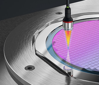
The Confocal Displacement Sensor CL-3000 Series is less constrained by the limited installation space inside the equipment.
Moreover, the sensor heads contain only lenses. They are not affected by heat or electrical noise yet still allow high-accuracy height measurements inside the equipment.

Gap measurement for slit coaters
Slit coaters (slit-type coating equipment) discharge the coating fluid from a slit nozzle and coat a uniform layer of fluid on glass substrates, resin substrates, films, or metal foils.
High-accuracy coating is required for LCD manufacturing processes and Fan-Out Panel Level Packaging (FOPLP) in the semiconductor industry. Even slight variations in the gaps between the slit nozzle and target on the right or left end directly affect the process, causing coating defects or defective products.
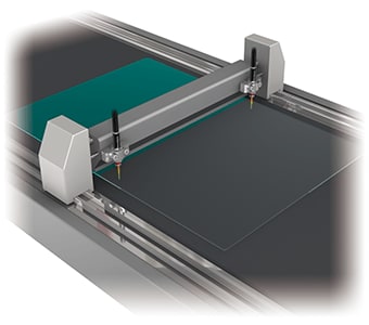
The sensor heads of the Confocal Displacement Sensor CL-3000 Series are extremely compact and lightweight compared to conventional heads. They are also not affected by heat or electrical noise, so they can be installed inside the equipment even when space is limited, ensuring high-accuracy and stable measurement.
Moreover, the CL-3000 Series can accurately differentiate the top and bottom surfaces of transparent objects with a thickness of 15 μm or more (such as glass substrates, transparent films, and thin layers of transparent materials), allowing for height (distance) measurement.
This enables accurate, simultaneous measurement of the distance from the slit nozzle to the surface of the glass substrate, and of the thickness of the substrate. Maintaining high-accuracy coating is also possible by sending the measurement results to the equipment for height control.
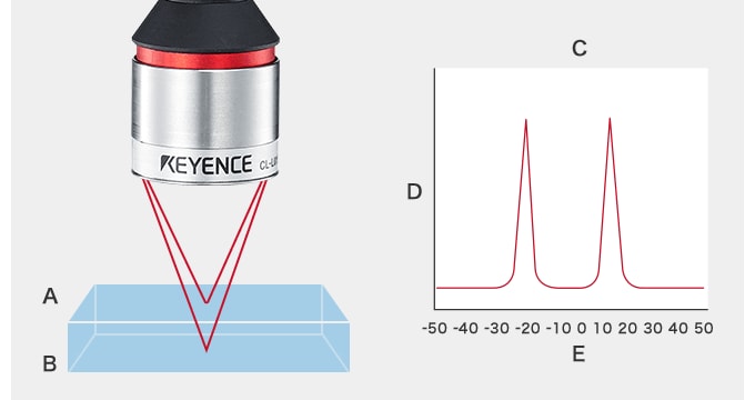
- A. Top surface
- B. Bottom surface
- C. Received light waveform
- D. Received light intensity
- E. Height (μm)
Column: Positioning of glass substrates
Conventionally, high-accuracy alignment of glass substrates has been done through image processing only. However, pre-alignment was necessary in order to improve processing times while maintaining high accuracy, but pre-alignment was problematic.
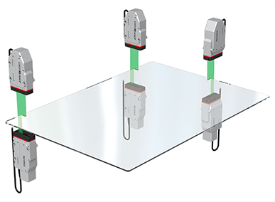
The High-speed Optical Micrometer LS-9000 Series provides a mode for measuring transparent targets in addition to a two-level edge detection threshold value setting. This enables stable measurement and positioning without being affected by the edge shape of the thin glass substrate.


