Electronic Component Inspection
Smartphones, tablets and other electronics have been designed to be smaller and thinner, and to use higher density components. As a result, the electronic components of such products have become more compact and precise in addition to having a more functional design. This led to an increase in sophisticated automatic coating such as bonding or potting precision components with super-small quantities of adhesive and precision coating of cream solder onto high-density PCBs.
Conducting 100% inspections of such precision coating requires high accuracy and stability as well as measurement speed capable of handling the takt time of the line. This section describes examples of effective adoption of displacement sensors for inline inspection of precision coating.

- 3D shape measurement of precision coating (High-Speed 2D/3D Laser Scanner)
- Height/volume measurement of precision coating areas (3D Interference Measurement Sensor)
3D shape measurement of precision coating (High-Speed 2D/3D Laser Scanner)
The High-speed 2D/3D Laser Scanner LJ-X8000 Series features a wide blue laser beam to allow high-speed measurement of 2D cross-sectional shapes without being affected by the material, glares, or surface conditions of the target. The LJ-X8000 also makes it possible to generate a 3D shape through image processing of the 2D cross-sectional shape data, enabling inspection for more minute coating defects.
Shape inspection of adhesive on CMOS
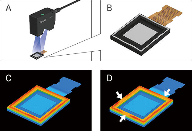
- A. Example measurement setup
- B. Measurement target (adhesive applied along the edge of a CMOS package)
- C. 3D image processing (Example of acceptable product: The height of adhesive is uniform.)
- D. 3D image processing (Example of unacceptable product: Varying heights are detected.)
In this process, adhesive is applied along the edge of a CMOS package for adhesion sealing with a glass substrate. Any defect in the height, position, or volume (applied amount) of the adhesive impairs the airtightness of the encapsulation and affects the performance and durability of the product.
Shape inspections based on 3D image processing that combines the High-speed 2D/3D Laser Scanner LJ-X8000 Series and an image processing system allow accurate inspection not only of the width or lack of adhesive but also of the height, which is difficult with conventional vision sensors. The ultra-high-speed sampling rate of 64,000 cycles/second can also be suitable for inline inspection with a short takt time.
Inspection of cream solder on PCB
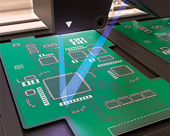
Conventional inspections after automatic cream solder coating on PCB land (PAD) before the reflow process are limited to checking the coating area with a vision sensor.
The LJ-X8000 Series can measure not only the area of coated cream solder but also its height, volume, and position at high speed. Accurate inspection even when the PCBs have components positioned at high densities is also possible.

Height/volume measurement of precision coating areas (3D Interference Measurement Sensor)
The assembly process of precision electronic components requires high-accuracy automatic coating of super-small quantities of adhesive by a dispenser robot. For inline inspection of small precision electronic components, displacement sensors that detect targets using points or lines require frequent stage movement, which may affect takt time.
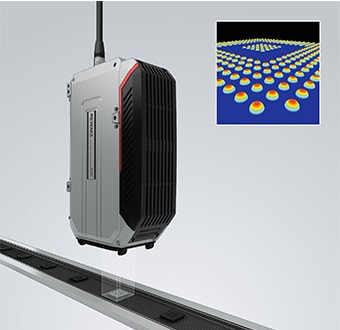
The 3D Interference Measurement Sensor WI-5000 Series can measure the height and volume of the area (surface consisting of multiple points) of applied or dispensed adhesive instantaneously, enabling high-speed and high-accuracy inline inspection.
The WI-5000 Series can detect 80,000 points of height data or area information per 10 x 10 mm virtually instantly (within up to 0.13 seconds). This is sufficient for ensuring high-speed 100% inline inspection.
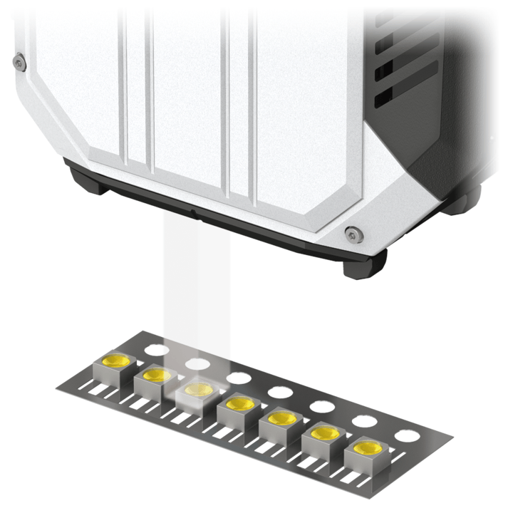
Height and volume measurement of small quantities of adhesive on precision components
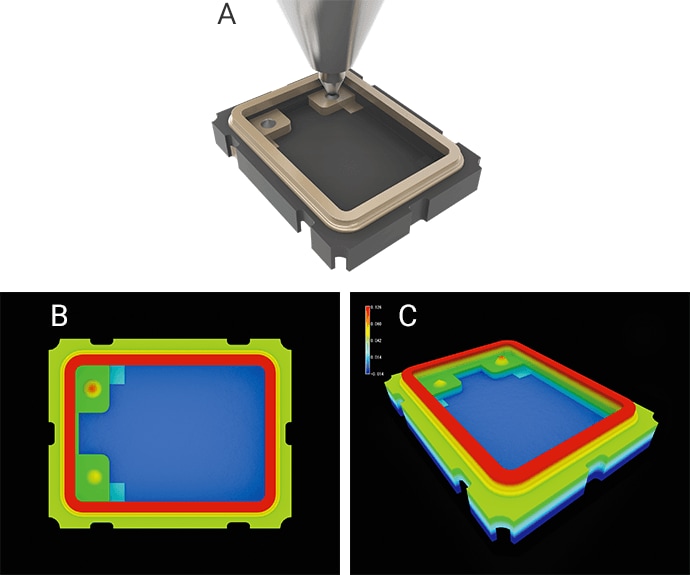
- A. Image of small quantities of adhesive on a crystal oscillator
- B. Result of 3D measurement (Example of unacceptable product: Variations in adhesive peak and height are detected.)
- C. Visual 3D shapes created from overhead height data measurements
The production of precision components such as small crystal oscillators requires the inspection of super-small quantities of adhesive immediately after coating. The WI-5000 Series can measure the height and volume of small adhesive quantities instantaneously with a measurement accuracy of 1 μm. This ensures high-speed 100% inline inspection.
With an emission of light with a wide dynamic range, the WI-5000 Series ensures stable measurement of targets with varying materials, colors, reflectance, and transparencies.
Even with deep targets such as component packages, the height of a surface (area) can be measured from above. Unlike conventional displacement sensors that measure points, measurement is not affected by unmeasurable areas caused by interruption of the reflected light or blind spots.
- Comparison of measuring areas between conventional displacement sensors and the WI-5000 Series
-
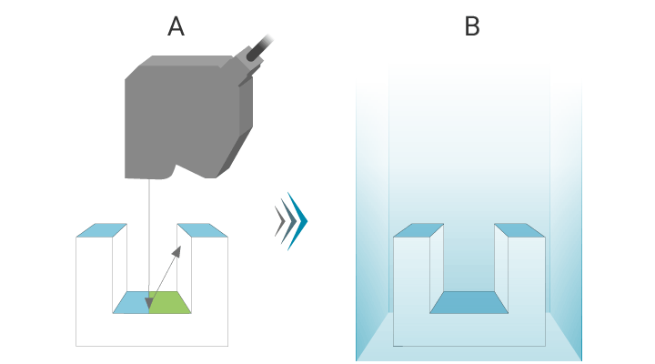
- A. Conventional displacement sensor
- B. WI-5000 Series
- Measurable area
- Unmeasurable area
Measurement of potting height on precision components
LEDs (Light Emitting Diodes) are used in various products such as lighting equipment or display backlights, so long-term reliability is essential. Potting is an important process that precisely dispenses resin with a dispenser in order to secure internal components or encapsulate modules.
Using the WI-5000 Series for inline inspection of LED potting ensures stable measurement of potting resin heights without being affected by the target material. Unlike typical displacement sensors, the WI-5000 Series instantaneously measures an entire area rather than a single point, resulting in simple and minimal target movement required for inspection.


