Accurately Measure and Analyze the 3D Shape of Warped PCBs
When mounting electronic parts and devices, PCBs are subject to stress due to bonding and heating during the reflow process. The reflow process achieves efficient component mounting, however stress due to heating may cause heat deformation of the PCB such as warpage, waviness, or strain. When a PCB is deformed, the joint strength of parts or fitting with the case may deteriorate, resulting in a serious effect on the yield rate.
This section explains basic knowledge about PCB deformation, problems with deformation measurement, and the latest measurement methods.
- Deformation of PCBs
- Simulation Analysis and Evaluation of PCB Deformation
- PCB Deformation Measurement and Evaluation Difficulties
- PCB Deformation Measurement Solutions
- Summary: Dramatic Improvement and Higher Efficiency for Deformation Measurement of PCBs
Deformation of PCBs
The surface of a PCB (Printed Circuit Board) should be flat so that it is possible to correctly mount components. However, heat deformation such as warpage or curvature may occur due to excessive stress caused by heat. The reasons why PCB deformation has increasingly become a problem and the effects of deformation are explained below.
PCB heat deformation
As a result of multi-layer and increasingly compact designs of PCBs which mount electronic components, as well as advances in high density mounting, the reflow method has been adopted as the primary method for mounting components. In the reflow process, solder paste (cream solder) is printed on the required parts, and bond for fixing the components is applied. Then the mounter places the electronic components onto the PCB. The PCB is then sent to an oven and heated to harden the solder or bond, resulting in efficient component mounting.
Due to the introduction of lead-free solder for environmental reasons, higher temperatures than before are now required for melting the solder in the reflow process. The higher temperatures inside the reflow oven increase PCB stress caused by heat. This has resulted in increased trouble such as warpage or curvature of the PCB in the high temperature oven.
Effects of PCB deformation
Deformation of PCBs can cause problems such as incorrect soldering due to deviated positions, or connection failures due to stress at soldered parts. When deformation is large, reduced fitting accuracy when installing the PCB into the casing may occur. These defects can largely reduce the yield rate.
When there is slight deformation in part of the PCB or the entire PCB, and it was installed into the casing and shipped without being noticed, product malfunctions due to electronic component connection failures may later occur and result in user complaints. In particular, control PCBs used in automobiles or airplanes require extreme quality control, as any malfunctions could be catastrophic. As a result, PCB shape is an important check item in the same way as lifting of the lead and solder fillet shapes.
Simulation Analysis and Evaluation of PCB Deformation
For improvements to eliminate PCB deformation, the heating conditions at each stage must be considered, verified, and evaluated. This must be done both during design and by actual heating evaluations.
Simulation analysis of deformation using software
At the PCB design stage, simulation analysis using CAD data may be performed. One method used to simulate and evaluate the behavior of a deforming object is FEM (Finite Element Method).
FEM (Finite Element Method)
Finite Element Method (FEM) is a simulation analysis method that divides a complex shape into shape elements until it becomes an aggregate of simple shapes, then finds the stress and deformation for each simple shape element. By stacking the individual simple shapes to recreate the entire original structure, stress and deformation can be predicted for each part of the entire object. By using CAD data of the target product in computer software, it is possible to conduct simulation analysis for factors such as rigidity, strength, vibration resistance, plastic deformation, breakage, and heat deformation.
Elements are classified by their shape as shown below.
| 0-dimensional element (scalar) |
 |
||
|---|---|---|---|
| 1-dimensional element (bar) |
 |
||
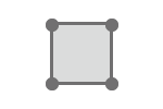
| 2-dimensional element (shell) |
 |
 |
|
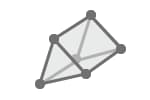
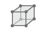
| 3-dimensional element (solid) |
 |
 |
 |
- 0-dimensional element (scalar): A point having no shape
- 1-dimensional element (bar): A line that is used to represent a part such as a bar, pillar, or beam
- 2-dimensional element (shell): Plane. Used to represent thin sheets and similar parts.
- 3-dimensional element (solid): There are three types of solid elements. In order from the left side, these are the pyramid-shaped tetra element, triangular bar-shaped penta element, and cubic hexa element. Using greater numbers of hexa elements can increase analysis accuracy for thick objects, however the level of difficulty is high and much calculation time will be required. On the other hand, advances in technology for automatically creating a 3D element mesh using tetra elements have reduced calculation times, and this method is suitable when prioritizing a reduction in time over accuracy.
Main features and flow of simulation analysis
As lower dimensions reduce the number of required shapes, the time required for analysis processing is shorter. When dimensions increase, although more time is required, higher accuracy data can be obtained. In the ordinary flow for deformation simulation of a 3D element PCB, first the design data of the PCB is divided into a mesh. Although nearly all PCB design data is 2D, some software requires conversion to 3D CAD format. For each element of the mesh, stress is applied by virtually raising the temperature as prescribed in the reflow process temperature profile, and the simulated data is acquired.
Requirements for PCB heating test and actual measurement/evaluation
Following the simulation, it is necessary to place the PCB into an actual reflow oven in order to verify that it behaves the same as the simulation under the proposed temperature profile.
Although it depends on the size, when a PCB is divided into 3-dimensional elements using the Finite Element Method, the number of elements may reach around 50 thousand. This means that unless the entire PCB surface shape is accurately measured, correct inspection results cannot be obtained no matter how detailed the simulation analysis is. Actual measurement is a very important process in order to ensure that all points which must be improved at the design stage are identified.
Next, we will explain problems with measurement using conventional measuring instruments, and the latest measurement system that is capable of evaluation by comparison with high accuracy computer simulations.
PCB Deformation Measurement and Evaluation Difficulties
With conventional measuring instruments it is difficult to accurately measure the entire PCB shape. Therefore, it is also difficult to quantify the sample shape and the changes it undergoes even when advanced simulations and experiments are performed. Some of the problems that users may encounter when using conventional measurement systems are outlined below.
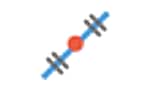
Measurement difficulties - profilometer
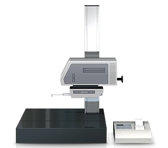
A profilometer measures and records the profile of a target by tracing its surface with a stylus.
In recent years, profile measurement systems have been developed that use a laser instead of a stylus to measure complex shapes by tracing the profile in a non-contact manner. Some models are even able to perform measurement of both the top and bottom surfaces.
Profilometers face the following challenges when measuring PCB deformation:
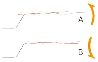
- A
- Upward slope
- B
- Downward slope
- Because the target is measured by tracing along lines, it is difficult to measure and evaluate deformation over a large area.
- It is not possible to identify the entire surface shape of the target.
- It is difficult to measure around mounted components on the surface.
- Setting a reference plane using lines is difficult, and as a result measurement error may occur (see figure).
Measurement difficulties - CMM
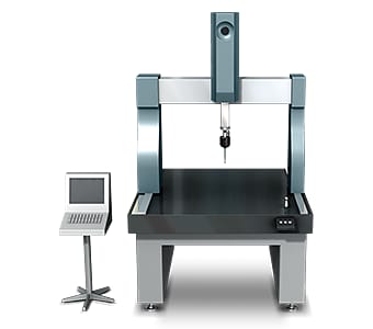
In general, when measuring PCB deformation using a coordinate measuring machine, it is necessary for the end of the probe to contact four or more corners on the measured surface of the target.
In case of a plate for example, generally six to eight points are measured. When the measurement area is large, measurement accuracy can be improved by increasing the number of measured points to collect more measurement data.
CMMs face the following challenges when measuring PCB deformation:
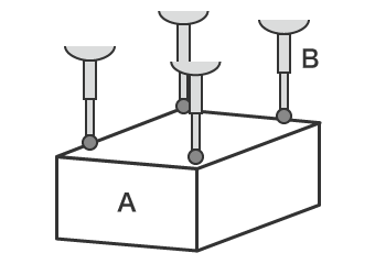
- A
- Target
- B
- Probe
- Because it is necessary to measure by contact at a limited number of points, it is impossible to identify the entire shape of the target.
- Measuring more points to acquire more measurement data requires much time, and it is not possible to identify the detailed shape of the entire target and locations of surface irregularities.
PCB Deformation Measurement Solutions
Conventional instruments only measure shapes using lines or points, and the entire shape of a deformed PCB cannot be identified. Furthermore, it is difficult to obtain the maximum and minimum values for every surface irregularity on the entire target, or to quickly make quantitative comparisons.
To resolve these measurement problems, KEYENCE has developed the 3D Optical Profilometer VR Series.
The VR Series accurately captures the 3D shape of the entire target surface without contacting the object. The VR Series does not require special fixturing or subjective decisions to be made, enabling accurate measurements to be performed by any operator.
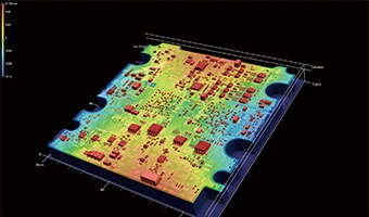
Advantage 1: Captures data across the entire surface in 1 second
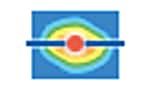
The VR Series can acquire surface data from 800,000 points with a single non-contact measurement in as little as one second. The maximum and minimum surface irregularities (height, depth) in the acquired 3D shape can be displayed in a color map to visualize the deformed locations on the entire target.
Because data is captured across the entire surface, profile lines can be drawn in any location to visualize and quantify the height changes.
Measurement data can also be overlayed and compared with CAD data, or with scan data from the PCB prior to heating so that the deformation can be fully understood.
This delivers a dramatic reduction in man-hours and improvement of work efficiency, as well as accurate measurement, comparison, and evaluation.


Advantage 2: Simple measurement operation
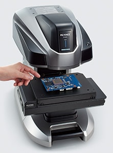
3D shape measurement can be performed easily just by placing the target on the stage and pressing a button.
By switching between the low magnification and high magnification cameras, accurate measurement of the entire PCB or detailed parts can be performed using a single system, even for small PCBs.
The VR Series incorporates the industry's first Smart Measurement function that detects the size and surface conditions of the PCB and automatically configures the scan range and conditions to capture the entire PCB surface.
A wide-variety of built-in assist tools makes it possible for accurate and repeatable measurements to be performed by even novice users. This makes it easy to increase the number of measured samples and perform trend analysis not only for verification testing and evaluation of designs and simulations, but also for measurement and inspection during commercial production.


Summary: Dramatic Improvement and Higher Efficiency for Deformation Measurement of PCBs
The VR Series can measure 3D target shapes accurately and instantaneously by high-speed 3D scanning without contacting the target. In addition to measuring the 3D dimensions of the entire PCB, this makes it possible to rapidly complete work that was previously difficult, such as measuring the shapes of minute height and surface irregularities, and comparing multiple data sets.
Using the VR Series resolves all of the measurement problems involved with conventional measurement.
- Height differences across the entire target can be visualized in the color map.
- Easily compare multiple sets of measurement data and apply conditions to multiple data sets at once, dramatically improving work efficiency.
- Once a scan is completed, profile measurement of any part and comparison of multiple data sets can be performed at any time.
- Without the need for positioning or other preparation, measurement can be done simply by placing the target on the stage and pressing a button. This eliminates the need to assign a specialized operator for measurement work.
- Because 3D shapes can be measured easily at high speeds with high accuracy, a large number of samples can be measured in a short time. This is useful for quality improvements.
In addition to R&D, design, and testing, it can be used effectively in a wide range of situations when manufacturing electronic products, including sampling inspection after the start of commercial production, and cause analysis when errors occur.

