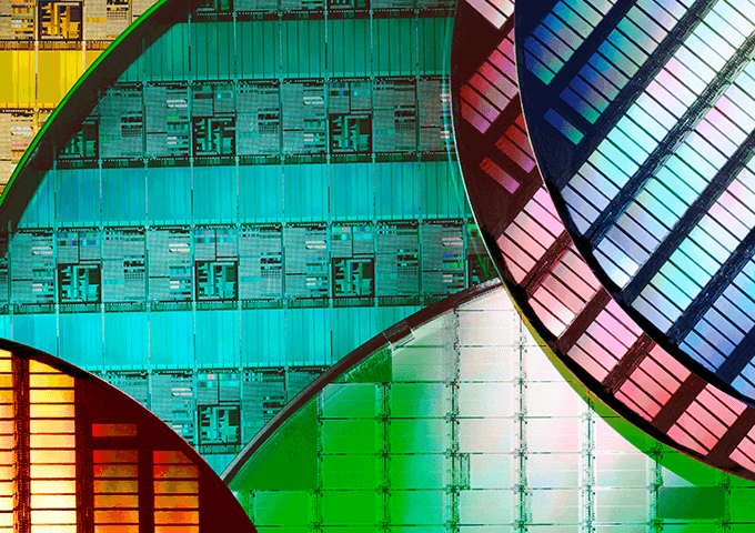
Semiconductor
Semiconductor devices such as ICs and LSIs are used in various kinds of electronic equipment and have been developed for improved density, performance, and miniaturization. Preprocessing in semiconductor manufacturing includes several processing steps for wafers, which are sliced from a single-crystal block (ingot) of silicon. Coating is used in many situations in the manufacturing process for surface processing, functionalization, and adhesion for processing.

- Adhesion in semiconductor manufacturing
- Functionalization and surface processing in semiconductor manufacturing (preprocessing)
Adhesion in semiconductor manufacturing
- Adhesion of semiconductor wafers and supporting glass plates
- During ultra-thin polishing of wafers, the wafer is bonded to a supporting glass plate with UV-curing liquid adhesive. The adhesive turns into a UV resin layer and comes off together with the glass plate after the process ends. (In addition to liquid adhesive, solid adhesives in tape form or sheet form are also used.)
Wafer adhesion/bonding requires a uniform coating of the adhesive.

Functionalization and surface processing in semiconductor manufacturing (preprocessing)
Coating plays an important role in various processing situations, including surface processing and resist coating or film-forming on wafers, which form the base for integrated circuits.
- Example of semiconductor wafer processing steps
- The following is a summary of the steps involved in processing single-crystal silicon wafers. Note that this is merely an example, and the actual steps may vary depending on the chips being manufactured.
This process is repeated before post-processing, where the chips are cut out from the wafer (dicing), connected to metal frames (lead frames) with gold wire (wire bonding), and encapsulated with resin sealant (molding).
Topic: Checking and maintaining the accuracy of processing equipment
In order to maintain processing accuracy and quality in the mass-production of semiconductors, it is necessary to maintain the accuracy of automatic processing equipment. Any inclination or improper hieght from placement or positioning of the wafer will greatly affect the processing quality. The compact Confocal Displacement Sensor can be placed inside wafer processing equipment to monitor for abnormal heights and inclinations of the wafers and improve processing quality.
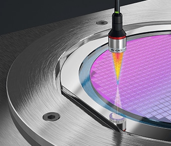
Introduction example: Wafer position check inside processing equipment


