The Instruction Cycle and How a CPU Executes Code

When estimating processing time in embedded software development, the basis is the very mechanism by which the CPU executes instructions.
Understanding the steps and process through which a single instruction is completed inside the CPU makes it easier to determine at the code design stage whether this processing will fit within the target processing time.
This article covers the flow of the instruction cycle and the main internal components of the CPU that support it.
- Why Embedded Software Developers Need to Know How CPUs Work
- Programs Are Arranged in Memory as a "Sequence of Instructions"
- Three Steps in Which the CPU Processes Instructions
- Key Internal Components of the CPU Supporting the Instruction Cycle
- Understanding the Instruction Cycle Helps Estimate Processing Time
Why Embedded Software Developers Need to Know How CPUs Work
To complete processing within the allotted time at a limited clock frequency, it is essential to understand how the CPU executes instructions. PC applications generally have ample clock speed and memory, and their required processing times are relatively long, so it is rarely necessary to focus closely on the number of clock cycles a single operation requires.
However, the situation is different for embedded software. This is because it is necessary to answer questions such as how many clock cycles a certain process will take to complete and whether wait states will occur in memory access during the design stage.
Assuming a process that continuously acquires sensor values at millisecond intervals, the number of clock cycles available for a single loop (repetitive processing) is very small, making it difficult to estimate the approximate processing time without knowledge of the instruction cycle. If implementation proceeds without this sense, processing delays are likely to be found during the testing phase, leading to rework.
Programs Are Arranged in Memory as a "Sequence of Instructions"

Source code written in C or other languages cannot be understood by the CPU as is. It only becomes ready for the CPU to handle after it is converted into machine language through the build process and laid out contiguously in memory, one instruction at a time. Program execution basically consists of following this sequence from the beginning and fetching and processing each instruction one at a time.
In embedded software, flash memory is used to store instructions. Flash memory may be built into the microcontroller or externally attached to it. Code on flash memory may be executed directly from flash memory, or it may be loaded into and run from RAM. Typically, it runs faster when loaded into RAM.
Since the read speed of flash memory directly affects the instruction retrieval speed, it is a factor that cannot be ignored when estimating processing time.

Three Steps in Which the CPU Processes Instructions
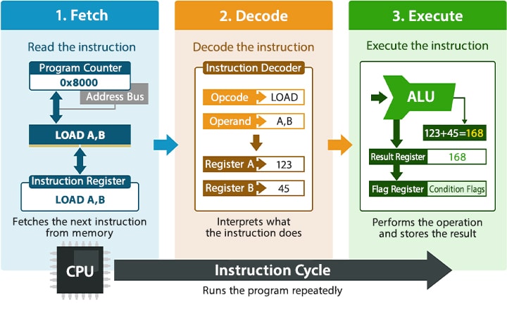
The CPU processes a single instruction in the following three steps. Although they may sound difficult just by their names, what they do is surprisingly simple.
- Fetch
- Decode
- Execute
This series of steps is the instruction cycle, and the CPU executes programs by repeating this cycle.
Fetch - The Program Counter Points to the Next Instruction
In fetching, an instruction is read from the memory address pointed to by the program counter and stored in the instruction register. The program counter is a register that always holds the address of the next instruction to be executed.
If the program counter is pointing to address 0x8000, the CPU reads the contents of address 0x8000 through the address bus and sends them to the instruction register. Once the read is complete, the program counter automatically advances to the next address, so at this point, preparation for retrieving the next instruction is complete.
Each time an instruction is retrieved, the counter advances. This repetition forms the flow of program execution.
Decode — Decoding the “what” and “where” of an instruction
During decoding, the instruction decoder decodes the opcode and operand contained in the instruction and sends control signals to each part of the CPU. The opcode indicates the type of operation (instruction), and the operand indicates the location of the target data (address).
For example, if an instruction to add the values of register A and register B is received, the opcode corresponds to addition, and the operands correspond to registers A and B. After reading this, the decoder instructs the ALU to execute the addition, while simultaneously preparing to retrieve data from the target registers.
Note that the ALU is an arithmetic unit inside the CPU. It is equipped with basic circuits for addition, subtraction, comparison operations, and logical operations, and processes data in general-purpose registers.
The decoding speed depends on the instruction set architecture of the CPU. Since the RISC architecture, which is widely used in embedded systems, has a fixed-length instruction format, the circuit structure of the decoder remains simple, making it easy to complete decoding in a single clock cycle.
Execute — The ALU executes the operation
During execution, the ALU executes the operation according to the instructions from the decoder and stores the result in a register.
Let’s assume a scenario where we determine whether the value obtained from a temperature sensor exceeds the upper limit. In this case, the ALU compares the sensor value stored in the general-purpose register with the preset threshold of 80°C 176°F, and the result is reflected in the flag register.
For addition or subtraction, the operation result itself is written back to the general-purpose register, but for comparison operations, the change in the flag is the main output. The next branch instruction looks at this result to determine whether to sound an alarm or continue reading the sensor value.
Such combinations of comparison and branching frequently appear in the control logic of embedded systems. It is worth keeping in mind that a single comparison instruction can take about three clock cycles.
Key Internal Components of the CPU Supporting the Instruction Cycle
The fetch, decode, and execute steps described above are made possible by the cooperation of multiple components inside the CPU. The key components that support the instruction cycle are as follows.
- Registers
- ALU (Arithmetic Logic Unit) and Buses
This section explains their respective roles and how they relate to the instruction cycle.
Registers — High-Speed Temporary Storage Area Inside the CPU
Although the capacity is extremely small compared to memory, registers are storage areas that the CPU can access in a single clock cycle. Since they are involved in every step of the instruction cycle, they can be considered the CPU's closest data storage locations.
Among the main registers, the three that directly appear in the flow from fetch to execute are the program counter, instruction register, and general-purpose registers. The program counter holds the next instruction address, the instruction register holds the instruction obtained by fetching, and the general-purpose registers hold the operands and results, respectively.
In addition, registers include flag registers that record the status of comparison operations and overflows, and stack pointers that manage the current position of the stack area.
Since the available RAM area is limited in embedded systems, it is important to pay attention to the design of the area pointed to by the stack pointer from an early stage.
ALU (Arithmetic Logic Unit) and Buses
As mentioned above, the ALU is an arithmetic unit inside the CPU that executes operations on data in general-purpose registers. The bus is the path that connects this ALU, registers, and memory to carry data and instructions.
There are three types of buses: address bus, data bus, and control bus. The address bus specifies the memory address to be accessed, the data bus carries the actual instructions and data, and the control bus transmits the type of operation, such as reading or writing.
In addition, there are two bus architectures: Von Neumann and Harvard. The Von Neumann architecture shares the bus for instructions and data, whereas the Harvard architecture has dedicated buses for each, allowing instruction fetching and data reading/writing to proceed simultaneously.
Since clock cycles are limited in embedded systems, the Harvard architecture, which allows these simultaneous operations, is widely adopted.
Understanding the Instruction Cycle Helps Estimate Processing Time
By understanding the instruction cycle, you can estimate the number of clock cycles required for processing at the code design stage. Although the CPU operates in synchronization with clock signals, the number of clock cycles required for a single instruction is not fixed.
This value is called CPI (Cycles Per Instruction); while a simple addition can be completed in a single clock cycle, instructions that require multiple internal steps, such as division, take several clock cycles or more.
In addition, a delay called a wait state may occur during memory access. A typical case is when reading instructions from flash memory, where the memory response cannot keep up with the operating speed of the CPU, resulting in an idle period of several clock cycles. When a cache is used, the processing time varies greatly depending on whether it is used or not. Unless these factors that create idle periods in processing time are carefully considered and investigated, the processing performance will change significantly.
In this way, estimating processing time achieves high accuracy only when including not only CPI but also these wait states. Whether this estimation can be made with high accuracy before running on the actual machine will significantly affect confidence in decisions at the design stage.
At the same time, it is also important to measure how much time it takes to process the implemented code at an early stage. Measuring the time on an actual microcontroller will show how much processing time margin is available.