Choosing Sleep Modes and Firmware Implementation Tips
The key to reducing power consumption in battery-powered embedded devices is not just hardware selection. It includes proper use of sleep modes, dynamic control of clocks and voltages, minimizing CPU active time using DMA, and actual measurement and verification with power profilers.
This means firmware developers have more control than one might imagine, and addressing these areas early in the design phase will reduce rework in later stages.
- Why FW Developers Should Lead Low-Power Design
- Types of Sleep Modes and How to Choose Them
- Dynamic Control of Clocks and Power Supplies
- Utilizing DMA, Interrupts, and Snooze Mode
- Power Consumption Measurement and Optimization Cycle
- Low-Power Design Pitfalls Checklist

Why FW Developers Should Lead Low-Power Design
In battery-powered embedded devices, power consumption is determined more by sleep transitions and clock management on the FW side than by hardware selection.
Indeed, looking at a certain microcontroller manual, the supply current, which flows up to 12 mA in normal mode, drops to 0.25 µA in software standby. This difference is huge, like leaving the faucet wide open and expecting the effect of a water-saving showerhead. Therefore, leaving it to the circuit designer is not an option.
However, when to enter standby and which peripheral modules to stop is a FW design decision. This is a subtle but highly effective area, and FW developers need to manage it at the peripheral level, including the selection of sleep modes, control of clocks and peripherals, and iterative improvements based on measurements.
Types of Sleep Modes and How to Choose Them
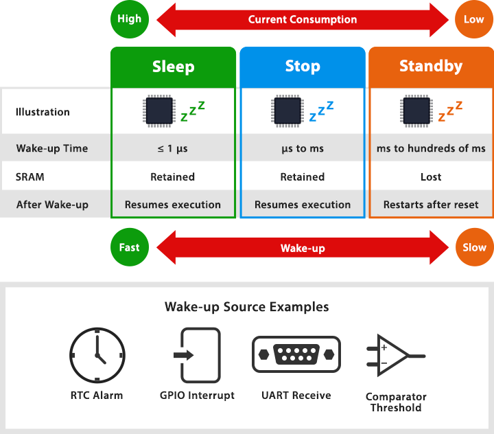
MCU low-power modes are divided into multiple stages from sleep to standby, and the lower the current consumption, the slower the recovery tends to be.
Therefore, it is quickest to choose based on the allowable recovery time; leaving this ambiguous will cause the design to become unsettled later.
Differences Between Sleep, Stop, and Standby
The ARM Cortex-M core has two low-power instructions, WFI and WFE, and switches between Sleep and Deep sleep using the SLEEPDEEP bit. Each vendor layers chip-specific modes on top of this; in the STM32 Series, SLEEP corresponds to Sleep mode, and DEEPSLEEP corresponds to Stop/Standby.
In Sleep mode, only the core is stopped while peripherals remain active, and recovery is as fast as 0.36 µs in the STM32L0. On the other hand, in Stop mode, most clocks are stopped, and recovery takes from µs to ms, but since SRAM is retained, processing can resume immediately.
Dropping down to Standby clears the SRAM, and recovery is equivalent to a reset. Since this boundary is difficult to change later, it is safest to use Stop as the default unless battery life is the absolute highest priority.
Selecting Wakeup Sources and Designing Recovery Time
First, narrow down the wakeup sources based on the application. For periodic events, use an RTC alarm; for external events, a GPIO interrupt; for communication standby, UART reception; and for analog monitoring, a comparator threshold. In this way, the required source determines the mode options.
A commonly overlooked aspect here is the clock configuration after recovery. In the STM32, the PLL is stopped when recovering from Stop mode, so a stabilization wait after restart is unavoidable when a high-speed clock is required. Note that this wait can be bypassed by specifying the internal RC oscillator (HSI) as the wakeup clock.

Dynamic Control of Clocks and Power Supplies
Sleep modes are not the only means of power saving. Even while the MCU is running, power consumption can be reduced by scaling down the clock frequency and power voltage.
Dynamic Frequency Scaling (DFS) and Voltage Scaling
If the clock frequency is lowered according to the processing load, dynamic power consumption decreases almost proportionally. In the RA2E3, the difference is 4.80 mA at 48 MHz versus 1.40 mA at 8 MHz. With MCUs like the STM32L that can switch internal voltage in steps using VOS, static current can be further reduced.
However, changing the frequency also affects the USART baud rate and other parameters, so the design of the switching timing is an area where you cannot cut corners.
Peripheral clock gating
Simply stopping the clocks of unused peripherals can visibly change the current consumption. In STM32, clocks for UART, SPI, TIMER, etc., can be individually turned ON/OFF using the RCC registers, but it is not uncommon for HAL initialization templates to enable them all at once by default.
Because you usually notice that “everything was left on” only during the measurement phase, you can reliably reduce power consumption just by reviewing the initialization code once.
Utilizing DMA, Interrupts, and Snooze Mode
Another axis for reducing power consumption is to shorten the time the CPU is awake. By using design patterns that delegate data transfers and monitoring to components other than the CPU, you can significantly increase the sleep ratio.
Maximize CPU sleep time with DMA transfer
The continuous conversion results of the ADC are transferred to SRAM via DMA, and the CPU is only woken up by an interrupt when the buffer is full. This is the basic pattern of “event-driven + DMA.” Even with UART reception, combining DMA with IDLE detection interrupts avoids waking up the CPU for every byte.
Furthermore, compared to a configuration that keeps the CPU running through polling without using these patterns, the difference in power consumption can range from 10 times to nearly 100 times depending on the design. Although it may seem like tedious wiring work, its impact on the sleep ratio is significant.
Snooze Mode: Making Decisions with Peripherals Alone Without Waking the CPU
In the snooze mode of the Renesas RA and RX Series, only the ADC operates intermittently during software standby, and the CPU is woken up only when the comparator determines that a threshold has been exceeded. This mechanism allows continuous monitoring to proceed at a standby-equivalent current consumption during periods when the CPU is not involved.
In STM32, a similar configuration can be built using LPTIM and ADC automatic injection, but the register setting procedures are quite different. Even though the concept is the same, the implementation needs to be adapted for each manufacturer.
Power Consumption Measurement and Optimization Cycle
Whether power consumption meets the design target cannot be fully determined by calculations or simulations alone. There are differences that only become visible when you place a probe on the actual device.
Visualization with a Power Profiler
To capture current changes in the µA to mA range over time, use one of the power profilers sold by several manufacturers. The basic usage is to display one cycle of sleep → wakeup → processing → sleep as a waveform and identify in which section unexpected current peaks occur.
Comparing the typical values in the datasheet with the actual waveform may reveal leakage current of several tens of µA that was invisible on paper. The cause is mostly forgetting to stop peripherals or floating GPIOs, but once it appears on the waveform, troubleshooting is quick.
Estimating Battery Life
The average current consumption is calculated as (Irun × Trun + Isleep × Tsleep) ÷ (Trun + Tsleep). For example, with a CR2032 (nominal 220 mAh), a Run of 10 ms in a 1 s cycle, Irun = 5 mA, and Isleep = 2 µA, the average is approximately 52 µA. 220 ÷ 0.052 is about 4200 hours, which calculates to approximately half a year.
However, due to self-discharge, temperature characteristics, and aging, it is safer to estimate the actual battery life at 70% to 80% of the calculated value. Even in battery life calculation tools, the default derating factor is often set to 0.7, and writing the calculated value as-is in the specification sheet may lead to trouble later.
Low-Power Design Pitfalls Checklist
We have compiled a list of points that are easily overlooked. Please use this for checking during design reviews or debugging.
- Are unused GPIOs left as floating inputs?
- Is the no-load current consumption (Iq) of the LDO dominating the sleep current?
- Are you measuring the current without disconnecting the debug connection (SWD)?
- Have you forgotten to send a shutdown command to external components before sleeping?
- Is a current on the order of µA constantly flowing through the pull-up resistor?
If even one of these remains, the sleep current will not decrease no matter how much you optimize on the firmware side. In situations where “the code is perfect but the numbers do not match,” it is best to go through this list from top to bottom first.