Optical Comparator (Profile Projector)
Critical Inspection & Quality Assurance of PCBs
Printed Circuit Boards (PCBs) are boards that generate conductivity for electrical connections within a larger component like a smartphone or electric vehicle. PCBs are quite small and have tiny components that sometimes even the naked eye can’t see. Even so, PCBs hold immense responsibility with their circuits, tracks, vias, and layers.
When manufacturing PCBs, visual and electronic PCB inspection ensures that the PCBs will function correctly. In this blog, we’ll focus on the value of visual PCB inspection and how to integrate it into your applications.
Why PCB Inspection Matters
PCB inspection matters because it prevents faulty products from entering the consumer market. Since PCBs are integrated into almost every industry—including ones with tight tolerances—defective PCBs have cost, reputation, and life-threatening consequences.
The electric vehicle industry relies on PCBs for powering vehicles. The medical device industry utilizes PCBs in life-saving devices. Electronics like smartphones are held together by the PCB storage and conductivity ability. Inspection upholds these quality expectations.

PCB Inspection Methods
Visual and electrical PCB inspection ensures functionality and identifies potential defects. Although the methods differ, visual and electrical inspection are both integral parts of quality assurance.
Visual PCB Quality Inspection
Visual inspections focus on identifying physical imperfections in the PCB. However, just because these imperfections are visual doesn’t mean it’s an aesthetic inspection. Rather, these defects reveal clues about the functionality of the board in its final product.
Physical attributes like thickness, roughness, dimensions, dents, scratches, holes, pitch, and positioning are evaluated with visual inspection. Technicians can use microscopes or vision inspection systems to inspect dimensional aspects.
Electrical PCB Quality Inspection
Electrical inspections assess the circuits, solder joints, and functionality of a PCB. These inspections involve tests that simulate future tasks for the PCB to ensure that it behaves as expected within a larger component.

PCB Inspection Equipment for Visual Inspection
PCB inspection equipment varies with software, optics, and detail. The four types of PCB inspection equipment we’ll focus on in this blog are Manual Visual Inspection (MVI), Automated Optical Inspection (AOI), Automatic Laser Test (ALT), X-Ray, and Multisensor Measurement Systems.
Manual Visual Inspection for PCB Inspection
MVI involves a technician inspecting a PCB with their naked eye or a magnifying glass. During the viewing, the technician manually compares a PCB’s joints and circuits with a design image.
Automated Optical Inspection PCB Equipment
An AOI system is automated PCB inspection equipment that uses high-definition cameras and diversified lighting options. The lighting is shone from different angles, brightnesses, and colors for a clear view of the PCB.
The camera, lighting, and integrated software work together to automate the visual inspection process. Instead of manual comparisons, the AOI automatically uses the design image to identify defects like missing components, misalignment, or solder joint issues.
This automated approach is crucial for finding issues that may be overlooked by manual inspection because of the limited optics. AOI equipment pinpoints surface, dimensional, and placement defects.
Automatic Laser Test PCB Inspection Equipment
Automated Laser Test (ALT) equipment uses lasers for visual inspection. The laser scans the PCB and the laser is reflected. The ALT system then analyzes the reflection position and uses that to measure the PCB height and alignment.
Automated X-Ray Inspection PCB Equipment
X-ray inspection uses X-rays to look beyond the first layer. The X-rays inspect solder, delamination, and voids in a PCB.
Since the solder is made of heavy metals and the substrate is light silicons, the X-ray waves are absorbed only by the solder. The solder absorbing the rays allows for an internal look at a PCB.
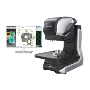
Multisensor Measurement System
A multisensor measurement system is an inspection device that combines optics, a touch probe, and a laser. These systems are used for PCB inspection because of the three-way expertise of combining the benefits of ALT and AOI with a probe. With these capabilities, multisensor systems are ideal for inspecting dimensions.

Choosing the Right Visual Inspection Approach
The right visual PCB inspection approach aligns with your board’s complexity, production volume, budget, and industry.
Board Complexity
The design, circuit, and layer complexity of your PCB all play a role in your approach. Single-sided PCBs will not require as detailed examination as dual or multi-layer. Therefore MVI may be an appropriate approach for single-sided PCBs.
Multi-layer PCB inspection requires internal inspection that can’t be achieved with the naked eye or just a microscope. Because of the complexity, multi-layer PCBs are compatible with X-ray, AOI, ALT, or multisensor measurement systems.
Production Volume
Reviewing your production volume and its alignment with automated versus manual systems is crucial for your approach. Large PCB production volumes benefit from AOI, ALT, and multisensor measurement systems because of the complete automation. Smaller PCB production volumes may not require the same investment into an advanced machine.
Budget
Although it's tempting to choose the novelty of an X-ray machine, the newer technology comes at a high cost. Likewise, MVI is more budget-friendly but will not offer the same level of precision or expertise.
When choosing your approach and weighing options against a budget, consider multi-sensor measurement systems. Multisensor measurement systems combine ALT and AOI methodologies into one machine.
Industry
Considering industry tolerances is necessary for your inspection approach. Even if your PCBs are single-layered or simple, strict tolerance industries like medical devices or EVs will need an advanced system.
Integrating PCB Inspection into Your Applications
Printed circuit board inspection needs top-tier quality assurance for medical, EV, aerospace, and electronics industries. Inspection is a win-win situation: your consumers get quality assurance while you build a quality reputation.
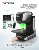
If you’re ready to integrate PCB inspection for your facility, KEYENCE can help. We specialize in multisensor measurement systems for automated PCB inspection.
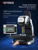
KEYENCE’s IM-X multisensor measurement system can inspect 5,000 locations on up to 1,000 PCBs simultaneously— meaning that inspection tasks are shortened in time and cost per inspection.
The IM-X autofocuses and does not need part positioning. The autofocus is specialized with a 20-megapixel CMOS camera, a multi-lighting system, and a laser that are ideal for detailed and layered PCBs. The camera captures tiny contrasting details with help from the multi-angle and multi-color illumination.
If you are ready to implement PCB inspection equipment, contact KEYENCE today.
Get detailed information on our products by downloading our catalog.
View Catalog