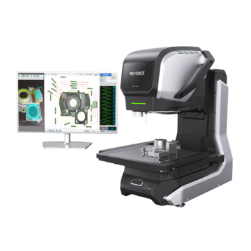
Optical Comparator (Profile Projector)
Semiconductor Quality Control
![]()
In our automated world, semiconductors serve as the backbone of many products and services. Semiconductors fuel the functionality of smartphones, electric vehicles, and computers with their data storage and energy control capabilities.
However, their seamless integration into products is not possible without quality assurance. Before a semiconductor is sent to the market, it must go through semiconductor quality control tests and inspections.
These tests and inspections scrutinize semiconductors from the raw wafer to the final product. Semiconductor inspection determines whether the semiconductor is eligible for use and reveals data about how the semiconductor functions. In this article, we’ll discuss how semiconductor quality control inspection and tests are conducted and how to incorporate a multisensor measurement system.
Let’s take a deeper look at the importance of semiconductor quality control, how the process works, and how to implement it into your applications.
What are Semiconductors?
Semiconductors are materials that have partial conductivity. The level of conductivity is between a metal and an insulator.
Usually made of silicon, semiconductors are the cornerstone of electronics. They ensure products like electric vehicles, computers, and smartphones have the electrical properties to operate.
We’re here to provide you with more details.
Reach out today!

Semiconductor Testing Process
Semiconductor Quality Control Inspection for Wafers
The first semiconductor quality control inspection is the wafer inspection.
The wafer is a thin slice of silicon with circuits built on top. Since the wafer is the foundation of semiconductors, this step is crucial to identify defects before the manufacturing process continues.
Manufacturers inspect for physical and functional defects. Physical defects include contamination, deformities, or incorrect dimensions. Functional defects include faulty circuits.
Semiconductor Quality Control Inspection for Dies
After the wafer is inspected, it is cut into smaller parts, known as a die or chip. Each die will be a part of an individual electronic device.
Manufacturers conduct semiconductor inspections for physical and functional defects in each die. Physically, the manufacturers look for contamination, deformities, incorrect dimensions, or processing problems. For functional inspections, manufacturers ensure that every die works correctly. Since the die is cut from a wafer, there may be new semiconductor quality control issues that arise from processing.
Semiconductor Quality Control Inspection for Semiconductor Packages
After the dies are finalized, they are put into a protective packaging material. The protective packaging material keeps the semiconductor long-lasting and compatible with the device.
Manufacturers inspect the package for any added contaminants or deformities from the packaging process. Additionally, the semiconductor quality inspection technician checks that the package is sealed adequately for use.
Final Semiconductor Quality Control Inspection
Finally, the semiconductor is assembled. Now, manufacturers inspect the semiconductor through functional, parametric, and reliability tests.
These tests are conducted with different types of technology. Some semiconductors include a Built-In Self Test (BIST), which can test itself. Other technicians use Automated Test Equipment (ATE) to inspect multiple semiconductors simultaneously. The ATE can include AI software and multisensor measurement devices.
Discover more about this product.
Click here to book your demo.

Key Tests in Semiconductor Quality Control
The key tests in semiconductor quality control are functional, parametric, and reliability testing.
Functional testing ensures the chip works correctly, parametric testing gathers data about the chip with different parameters, and reliability tests a chip’s withstanding against environmental factors.
Functional Semiconductor Testing
Functional testing verifies that the semiconductor is working properly. These tests are applied by putting the chip through future functional scenarios and making sure it acts accordingly.
Parametric Semiconductor Testing
Parametric testing involves testing parameters such as voltage and current. The tested measurements are to ensure that these features are within the correct parameters and work in different conditions.
This type of testing is gaining popularity as semiconductors become more complex. Testing each parameter instead of the semiconductor as one unit gives more detailed intel into the semiconductor’s function.
Reliability Semiconductor Testing
Reliability semiconductor testing assesses a semiconductor’s durability against varying environmental conditions.
For example, a semiconductor that will be inside of a smartphone may go through a water resistance test. The test will determine how far the semiconductor can be submerged in water before breaking.
Contact us to learn more about how our advanced technology can help take your business to the next level.
Contact Us
Multisensor Inspection Semiconductor Applications
Multisensor measurement systems are measurement and inspection devices that use at least two sensors: camera, touch, and lasers.
These devices combine coordinate measuring machine (CMM) probe capabilities and optical comparator visual abilities. A multisensor system for semiconductor inspection excels at inspecting a variety of dimensional attributes.
Semiconductor Inspection for Surfaces
Wafers, dies, packages, and final semiconductors all require surface inspection. Surface inspection looks for contaminants, irregularities, and physical problems.
Contaminants, irregularities, and other physical problems are signs that the semiconductor may not be functional either by itself or when finalized into a product.
A ultra-high resolution microscope uses a high-depth camera and lighting to capture a microscopic image of the area and find any physical deformities. The lighting and camera are capable of detecting defects that are invisible to the naked eye.
At KEYENCE, our ultra-high resolution microscope for semiconductor inspection combines a large depth of field with high resolution to deliver a new level of observation. In addition, using optimal shadow effect mode, you can easily interpret images with a height color map.
Semiconductor Inspection for Dimensions
Wafers, dies, packages, and final semiconductors need dimensional inspection to ensure they fit within design specifications. Nonconforming dimensions may cause issues with assembly or functionality.
A multisensor measurement system uses a camera, probe and laser to measure dimensions. The probe traces the semiconductor dimensions and GD&T features and measures roundness with little force.
Using multisensor measurement for semiconductor applications is a type of ATE that specializes in inspecting multiple semiconductors at once. At KEYENCE, our multisensor measurement systems measure up to 5,000 locations on 1,000 semiconductors simultaneously.
Implement Semiconductor Quality Control Into Your Applications
Semiconductors are integral to the advancement of technology. These small parts are controlling energy flow and storing data. With semiconductors having a responsibility to technology, they must go through inspection. Using a high-resolution microscope and a multisensor measurement for semiconductor applications is best for tackling physical and dimensional inspections at a high degree of accuracy.
KEYENCE’s IM-X multisensor measurement system inspects 5,000 locations on up to 1,000 parts simultaneously. This means inspection tasks are shortened in time and cost per inspection. Our systems are specialized with a 20-megapixel CMOS camera and low-pressure probes ideal for detailed and fragile semiconductors. In addition, the white confocal laser can inspect height and depth dimensions instantaneously.
The best part? There’s no training required. The IM-X autofocuses and does not need positioning.
If you are ready to implement semiconductor quality control and then expedite the process, contact us today.
Get detailed information on our products by downloading our catalog.
View Catalog


