
Spectral-Interference Wafer Thickness Meter
SI-F80R series
Spectral-Interference Wafer Thickness Meter SI-F80R series
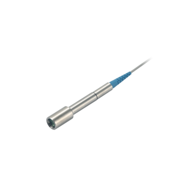
With the adoption of the near-infrared SLD, thickness measurement for the wafer alone is possible even while BG tape is affixed. Even when there is strong pattern-based variation on the surface of the wafer, accurate in-line measurement is possible. The SI-F80R Series features an extremely small size, lightweight, and heat resistant design, which allows the head to be installed in places that can’t accommodate conventional sensors. Furthermore, the construction of the head itself provides incredibly accurate measurements, as it isn’t susceptible to heat generation nor influenced by electromagnetic noise.
Features
- Wafer thickness can be measure even if back grinding tape is affixed
- Minimal pattern influence
- In-line measurement is possible
- Automatically maps the distribution of thickness for the entire wafer
