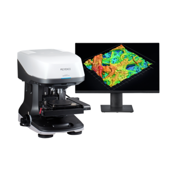
3D Optical Profiling Microscope
What Is a Laser Microscope? Technology, Applications, and How to Choose
Key Takeaways
- A laser microscope generates 3D surface maps and color images without contacting the sample.
- Confocal platform rejects out-of-focus light, enabling precise height measurement and sharp imaging on complex surfaces.
- One system replaces an optical microscope, surface roughness gauge, and 3D measurement tool.
- Applications span electronics, automotive, medical devices, semiconductors, and research — anywhere surface quality drives decisions.
- Compared to contact profilometers and SEMs: faster, no sample prep, no damage risk, quantitative 3D output.
This page covers everything you need to know about laser microscopes: how they work, what makes confocal technology effective, where they are used across industries, and how they compare to other measurement tools. Whether you are evaluating your first system or looking to upgrade an existing process, the sections below will help you make a confident decision.
What Is a Laser Microscope?
A laser microscope is a non-contact measurement instrument that uses two light sources — a laser for capturing height data and white light for capturing color information — to produce a high-resolution, three-dimensional surface map alongside detailed color imagery. By scanning the laser across the sample surface in the X, Y, and Z directions and measuring reflected light intensity at each point, the system achieves nanometer-level height resolution suitable for profile measurement, surface roughness analysis, and film thickness characterization.
What distinguishes a laser microscope from conventional optical tools is the range of information it delivers in a single measurement. The combination of a 3D height map, high-contrast intensity image, and full-color optical image effectively consolidates the capabilities of an optical microscope, scanning electron microscope, and surface roughness gauge into one platform. Measurements are performed in ambient conditions, which means no vacuum chamber, no conductive coating, and no sample preparation required. The system can also image the surface layer, interior structure, and bottom layer of transparent targets, enabling film thickness measurement on coatings, resists, and other materials that would normally require separate systems to evaluate.
How Does a Laser Scanning Microscope Work?
A laser scanning microscope builds its surface image one point at a time. The laser sweeps across the sample in a precise grid pattern, collecting reflected light data at each position rather than illuminating the entire field simultaneously. This point-by-point acquisition eliminates interpolation, ensuring that every surface detail in the final map is directly measured, not estimated.
The Confocal Principle
The accuracy of laser scanning microscopes depends on the confocal optical principle, which uses a pinhole positioned directly in front of the light-receiving element to filter out any light that does not originate from the current focal plane.
The measurement process works as follows:
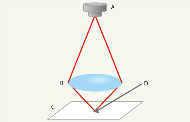
1. Laser Focus
The laser light emitted from the light source is concentrated at the focal point by the objective lens, illuminating a single point on the sample surface.
A: Light source
B: Objective lens
C: Target
D: Light emitted from the laser is concentrated on the measurement surface by the objective lens.
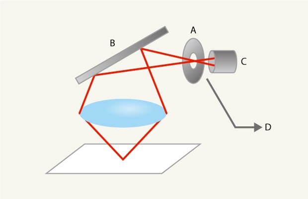
2. Reflected Light Detection
The reflected light travels back through the objective lens and is redirected by a half mirror toward the pinhole and detector. Because the pinhole sits at the conjugate focal point, only light reflected from the correct depth passes through cleanly.
A: Pinhole
B: Half mirror
C: Light receiving element
D: The reflected light is concentrated on the receiver by the objective lens.
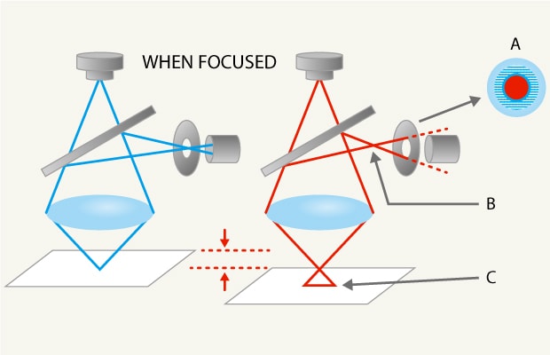
3. Out-of-Focus Light Rejection
When the objective lens is positioned above or below the focal plane, the reflected light spreads out before reaching the pinhole. The expanded spot cannot pass through, which dramatically reduces the signal from those depths and isolates only in-focus data.
A: The reflected light that enters the hole passes through, but other light is blocked by the mask shaded) part.
B: The light reflected from the target is focused at a position offset from the pinhole in the direction of the optical axis, so the spot expands such that the light is out of focus at the pinhole position.
C: The light concentrated on the target surface spreads out.
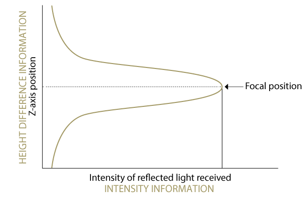
4. Z-Axis Scanning
The objective lens moves incrementally through the full measurement range along the X-, Y-, and Z-axes. At each position, the system records both the reflected light intensity and the corresponding height. The surface height at each pixel is identified as the Z-axis position where reflected intensity reaches its maximum.
By stacking these focal positions across the entire measurement field, the system generates three simultaneous outputs: a high-contrast laser intensity image, a full-color image with an extended depth of field, and a complete 3D height map of the surface.
What Are the Key Benefits of Laser Microscopes?
The practical advantages of laser microscope technology follow directly from how these systems are built and how they operate.
Ease of Use
Laser microscopes operate with the same accessibility as conventional optical microscopes. There are no vacuum chambers to establish, no conductive coatings to apply, and no meaningful sample preparation standing between an operator and a measurement. Users at any experience level can produce reliable, repeatable results with minimal setup time.
Depth of Field and Image Quality
This is where laser scanning technology most clearly outperforms standard optical microscopy. A conventional microscope illuminates the full field at once, which limits depth of focus and produces blur on surfaces with significant height variation. A laser microscope builds a fully focused composite image by tracking which pixels reach peak intensity at each Z-axis position, producing sharp, detailed images across the entire surface regardless of topography. It works just as effectively on a flat, smooth surface as it does on something heavily textured or complex.
Surface Roughness Measurement
Measuring surface topography is a core capability enabled by the small laser spot diameter. The spot is significantly smaller than the contact tip of a stylus profilometer, allowing accurate measurement of small grooves, textured finishes, and micro-scale geometries without any physical contact or risk of deformation. Roughness values are output as quantitative data, ready for direct comparison against specifications.
Material Versatility
Laser scanning microscopes deliver consistent, high-quality surface data across polished metals, soft polymers, glass coatings, composite materials, and transparent films without reconfiguration or surface preparation. For transparent targets, the system can measure not just the top surface but the interior and bottom layers as well, enabling film thickness measurement on coatings and layered structures that would otherwise require destructive cross-section techniques.
| Capability | Detail |
|---|---|
| Vertical resolution | Nanometer-level |
| Depth of field | Large; sharp imaging across high-variation surfaces |
| Outputs | 3D height map, high-contrast intensity image, full-color image |
| Contact required | None |
| Sample preparation | None |
| Transparent material measurement | Yes, including film thickness and layer structure |
| Operating environment | Ambient conditions; no vacuum required |
Laser Microscope Applications by Industry
Laser microscope applications are found wherever precise, non-contact surface characterization supports quality control, process development, or failure analysis. The combination of speed, resolution, and material flexibility makes these systems practical across R&D labs, quality departments, and manufacturing environments.
Automotive and aerospace production rely on laser microscopes to verify that machined components meet tight dimensional tolerances before they move to assembly. These systems can measure coating thickness on structural metal parts, track wear progression on cutting tools, and assess texture uniformity on sealing surfaces — tasks that would otherwise require multiple instruments and more time.
Medical device manufacturing depends on accurate surface topography measurement to ensure that implant surfaces meet the roughness specifications that govern tissue integration and regulatory compliance. Because the measurement is entirely non-contact, the finished surface is left completely unaltered during inspection, which is a critical requirement for parts that have already completed final processing.
Semiconductor fabrication uses laser scanning microscopes to examine wafer surfaces, detect particle contamination, and verify thin-film deposition uniformity across complex material stacks. The resolution and repeatability demand at semiconductor scales are about as tough as it gets in any industry, and laser scanning microscopy handles them without the destructive sample preparation that electron microscopy typically requires.
Research and failure analysis applications span laboratory characterization of fracture surfaces, thin-film morphology studies, and before-and-after comparisons of treated material samples. The ability to capture both visual and dimensional data makes the laser microscope particularly effective for failure investigations, where understanding what a surface looks like and what its dimensions are often needed to happen in the same step.
The KEYENCE VK-X4000 Series are one example of a platform designed to address this full range of industrial and research surface measurement demands.
How Does a Laser Microscope Compare to Other Measurement Technologies?
Choosing the right measurement tool depends on the application. The table below summarizes how laser microscopes compare against the most common alternatives.
| Feature | Laser Microscope | Contact Profilometer | Scanning Electron Microscope | White-Light Interferometer |
|---|---|---|---|---|
| Measurement Method | Non-contact optical | Physical stylus contact | Electron beam | Non-contact optical |
| Data Output | 3D surface map + color image | Single-line 2D profile | 2D image (3D requires additional steps) | 3D surface map |
| Sample Preparation | None | None | Often requires conductive coating | None |
| Operating Environment | Ambient | Ambient | Vacuum required | Ambient |
| Soft or Delicate Materials | Yes | Risk of marking or deformation | Risk of coating damage | Yes |
| Transparent Material Measurement | Yes | No | No | Yes |
| Vertical Resolution | Nanometer range | Nanometer range | N/A (imaging only) | Sub-nanometer |
| Surface Type Range | Wide, including steep slopes | Limited by stylus geometry | Limited by vacuum and coating | Best on smooth, flat surfaces |
Contact profilometers drag a physical stylus across the surface in a single straight line, and that limitation shapes everything about what they can and can't do. On soft, sticky, or delicate materials, there's a real risk the stylus damages the very surface you're trying to measure. Steep sidewalls and undercut features tend to cause problems too, since the tip simply can't follow those geometries accurately. But perhaps the bigger issue is that you're only ever getting one cross-sectional slice of the surface at a time. If a defect or a critical feature happens to sit just outside that line, you'll miss it completely, and you won't necessarily know you missed it.
Scanning electron microscopes can produce incredible images, but getting to that point takes real effort. Every sample needs to be coated with a conductive layer first, and the whole measurement happens inside a vacuum chamber. On top of that, what you get out is a 2D image. If you actually need height data, you're looking at additional techniques like stereophotogrammetry or ion beam cross-sectioning. For teams that just need quantitative 3D surface measurements on a regular basis, the prep work and equipment overhead add up fast.
White-light interferometers achieve sub-nanometer vertical resolution and perform exceptionally well on smooth, flat, or gently curved surfaces. Their limitation is sensitivity to surface conditions: rough textures, steep slopes, and materials with inconsistent or low reflectivity can all degrade measurement quality. Laser microscopes handle a much wider range of surface types while still delivering comparable vertical resolution for most industrial work, which in practice makes them the more flexible option when you're dealing with varied part geometries day to day.

Frequently Asked Questions
What Is a Laser Microscope?
A laser microscope is a non-contact surface measurement instrument that uses a focused laser to scan a surface point by point, measuring reflected light intensity to generate a 3D height map alongside a high-resolution color image. It combines the functions of an optical microscope, surface roughness gauge, and 3D measurement system in a single platform that operates at room temperature without sample preparation.
What Is the Difference Between a Laser Microscope and a Confocal Microscope?
A confocal microscope is a specific type of laser microscope that uses a pinhole to block out-of-focus light and isolate signal from a single focal plane at a time. All confocal laser microscopes are laser microscopes, but not every laser microscope uses the confocal principle. The confocal design improves imaging clarity and height measurement accuracy, particularly on rough or complex surfaces where stray light from adjacent depth planes would otherwise reduce measurement quality.
How Accurate Is a Laser Microscope for Surface Roughness Measurement?
KEYENCE laser microscopes achieve height resolution in the nanometer range. The small laser spot diameter enables accurate measurement of fine surface features, including small grooves and textured finishes, without touching or deforming the sample. This level of precision is generally superior to contact stylus profilometers for detailed surface characterization, and the non-contact approach removes the risk of altering the surface during measurement.
What Is the Difference Between a Laser Microscope and a Scanning Electron Microscope for Surface Analysis?
A scanning electron microscope provides exceptional magnification and image detail, but it requires a vacuum environment and often demands conductive coating of the sample before use. It also generates 2D images by default, with quantitative height data requiring additional processing. A laser microscope captures quantitative 3D surface data in an ambient setting with no sample preparation, making it significantly faster and more practical for production and quality control environments. For most industrial surface analysis applications, a laser microscope is the more efficient and non-destructive choice.
What Industries Use Laser Microscopes?
Laser microscopes are used across semiconductor manufacturing, automotive production, medical device manufacturing, aerospace, electronics, and precision tooling, as well as in materials research and failure analysis laboratories. Any industry where surface finish, texture, or topography directly affects part performance, regulatory compliance, or process control is a strong candidate for laser microscope integration.
Can a Laser Microscope Measure Transparent Materials?
Yes. Laser microscopes can observe and measure the surface layer, interior structure, and bottom layer of transparent targets, enabling film thickness measurement on coatings, resists, and other layered materials. This capability is particularly valuable in semiconductor and optics applications where layer thickness must be verified non-destructively.
How Does Laser Scanning Microscopy Differ from Standard Optical Microscopy?
Standard optical microscopy illuminates the entire field of view simultaneously, which limits depth of focus and produces blur on surfaces with significant height variation. Laser scanning microscopy builds the image one point at a time using a focused laser and the confocal principle, rejecting out-of-focus light at each position to achieve superior depth discrimination and image clarity. The critical distinction is that laser scanning microscopy generates quantitative 3D height data, whereas standard optical microscopy produces only 2D visual images without dimensional measurement capability.