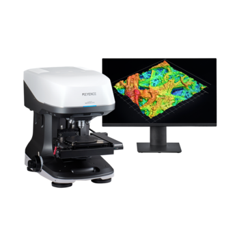
3D Optical Profilometers
White Light Interferometers for High-Precision Surface Measurement
Key Takeaways
- White light interferometers measure surface topography using optical interference for extremely precise non-contact analysis.
- White light interferometry is well-suited for detecting microscopic height variation, roughness, and nanometer-level features.
- These systems support high-resolution 3D surface measurement for precision manufacturing and material analysis.
- Compared with other surface measurement methods, white light scanning offers incredibly high accuracy over flat surfaces with small 3D features.
This guide covers the fundamentals of white light interferometry and how it achieves nanometer-level precision. You'll learn about interference principles, system capabilities, measurement considerations, and when this technology provides advantages over alternative profiling methods.
What Is a White Light Interferometer?
A white light interferometer measures surface height by analyzing patterns created when light waves interact. The system splits a light beam into two paths—one reflects off a reference mirror while the other bounces off the sample surface. When these beams recombine, they create interference patterns that reveal height variations across the surface.
This optical approach captures topography without touching the sample. The technology works particularly well on smooth, reflective surfaces where interference patterns form clearly. Engineers use these instruments to measure film thickness, surface roughness, step heights, and other features requiring nanometer or sub-nanometer precision in semiconductor, optics, and materials research applications.
Principles of Light Interferometry Explained
Light interferometry depends on wave behavior. When two light waves meet, they either reinforce or cancel each other based on their relative phase. If the optical path difference equals a whole number of wavelengths, the waves strengthen. If the difference equals a whole number plus half a wavelength, they weaken.
This creates the bright and dark bands visible in interference patterns. By counting fringes and analyzing their intensity, the system calculates surface topography. Phase shifting techniques improve precision by capturing multiple images at slightly different optical path lengths.
White Light Interferometers
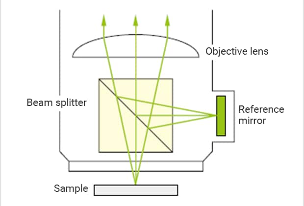
Light from the source is split by a beam splitter into two beams: a reference beam directed toward a reference mirror, and a measurement beam directed toward the sample surface. Both beams are reflected back to the beam splitter, where they recombine. The recombined beams travel to the image sensor, where their phase differences produce an interference pattern. Because white light has a very short coherence length, strong interference fringes only appear when the optical path lengths of the two beams are nearly equal. This property is what allows the system to extract precise height information across the sample surface.
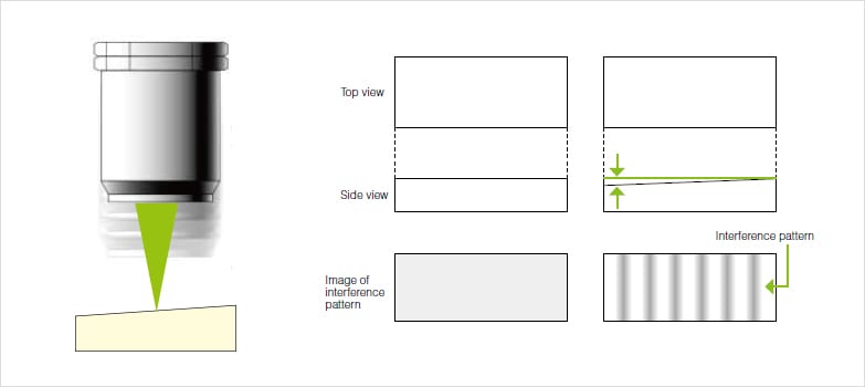
The white light interferometer is designed so that the optical path length from the imaging sensor to the reference mirror and that from the imaging sensor to the sample surface are the same. The asperity on the sample surface causes these path lengths to be unequal, which results in forming an interference pattern at the imaging sensor. The number of lines in the interference pattern is translated to peaks and valleys (heights) on the sample surface.
Cause of Light Interference
Light interference occurs when two light waves collide, causing each to strengthen or weaken. This section describes the interference of two lights reaching point P at a certain distance from the surface of the target. If the difference in distance between the two light paths S1P and S2P is an integer multiple of the light wavelength λ, the two light waves will strengthen and become brighter at point P due to the wave peaks overlapping. If the optical path difference is an integer multiple of the wavelength λ + 1/2 the wavelength λ, the peaks and valleys of the waves will overlap, causing the waves to weaken and become darker.
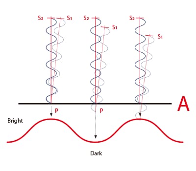
A: Optical path difference = S2P – S1P
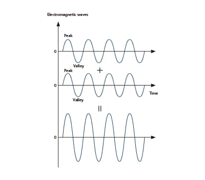
Optical path difference and light interference
When the optical path difference is an integer multiple of the wavelength λ
Strengthening due to peaks overlapping with peaks and valleys overlapping with valleys.
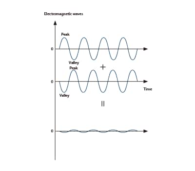
Optical path difference and light interference
When the optical path difference is an integer multiple of the wavelength λ + λ/2
Weakening due to peaks overlapping with valleys.
Interference Stripes
The interference light becomes lighter and darker at intervals equal to half the wavelength of the light source (λ/2). These patterns of light and dark are called interference stripes. The height of a target can be determined by counting the number of interference stripes.
The physicist Christiaan Huygens and others have proved that interference stripes of light form a graph (waveform) with a fixed period, as in the figure below. Optical interferometers use this physical phenomenon to ensure high-resolution measurement even at low magnifications.
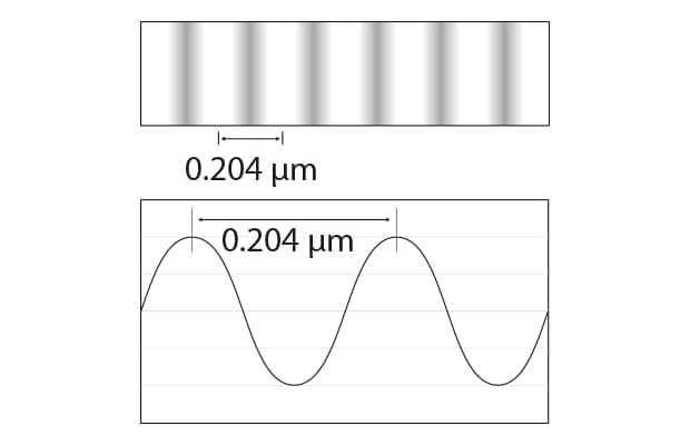
Interference stripe wavelengths
In this example, when using a 408 nm light source, the interference stripe spacing (wavelength) is 0.204 μm.
This value represents the height difference of the measured surface.
Because the height difference from peak to peak in the waveform graph is 0.204 μm, a resolution of 0.1 nm is possible by dividing the waveform graph into 2000 segments between the peaks.
Optical interferometers measure changes in height by measuring the changes between light and dark in regular interference stripes.
Phase Shift Interferometry (PSI)
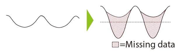
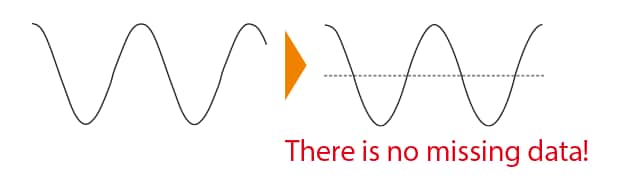
Determining whether the shape of the target is on an upward or downward slope is not possible when using interference stripes generated from a single-wavelength light source. However, this problem can be solved using phase shift interferometry.
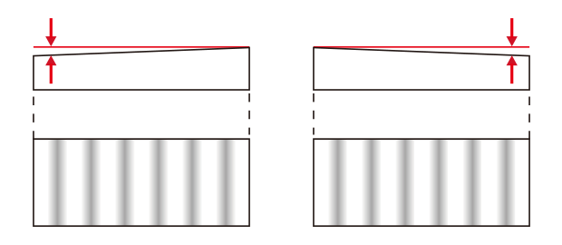
As shown in the figure to the left, the interference pattern from a single-wavelength light source is the same for both upward and downward slopes, making it impossible to determine the direction.
To solve this problem, the height is measured by capturing four interference stripe images as the objective lens and target are moved by λ/8 (1/8 wavelength) of the light source. This measurement method is called phase shift interferometry (PSI).
The Main Features of Phase Shift Interferometry Are as Follows:
- High-resolution Å (angstrom) order measurements are possible.
- The measurement time is short.
Reason for Using White Light as a Light Source
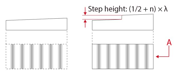
Appearance of interference stripes
A: The interference stripes are the same, even though the heights are different.
Measurement Using a Single-Wavelength Light
As shown in the figures to the left, with a height difference of (1/2 + n) × the wavelength λ of the light source, no changes are noticeable in the interference stripes, so determining the correct height difference is not possible.
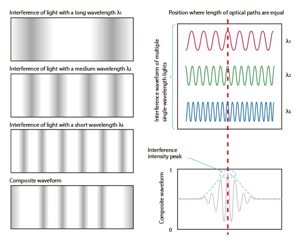
Composite interference stripes
Measurement Using White Light
When using a white light source, the interference stripes on the measurement surface at the focal point of the objective lens become stronger, and disappear when moving away from the focal point. Using a composite waveform created by superimposing interference stripes of different wavelengths makes it possible to detect the interference intensity peaks.
Measurement of Uneven Surfaces
KEYENCE's 3D Optical Profiling Microscope with a built-in white light interferometer uses a white LED to determine the interference stripe intensity at each height interval by moving the objective lens. Height information from the focal point position is obtained by using a linear scale to measure the lens position at the point where the interference stripes become stronger. This method is called vertical scanning interferometry (VSI).
Linear Scale Module
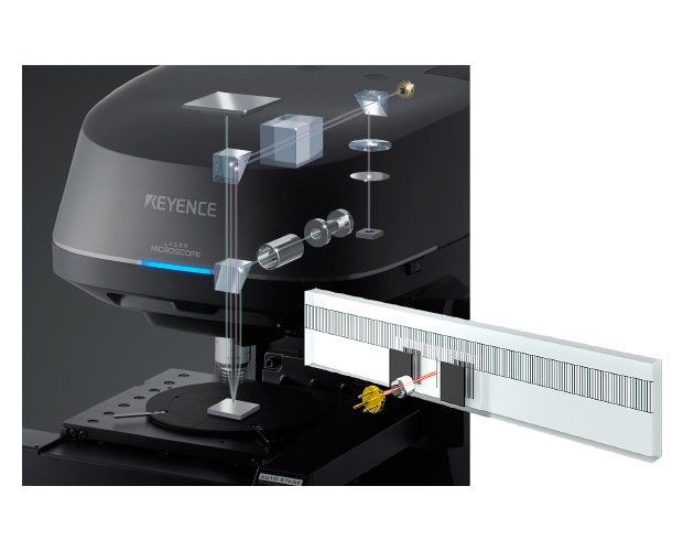
Objective Lens Scanning and Interference Stripe Intensity
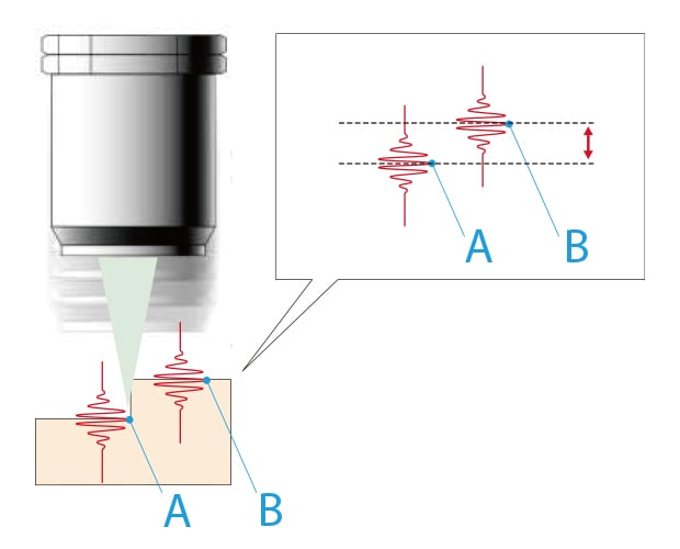
The difference between the interference intensity peaks at points A and B indicates the height difference.
High-Accuracy Measurement Even at Low Magnifications
Unlike many optical measurement techniques, the height resolution of an interferometer is independent of the magnification of the objective lens. This is because the composite waveform representing interference fringe intensity can be accurately reconstructed through calculation, even when the objective lens has a large depth of field.
Interference fringes appear at regular, predictable intervals due to the constant wavelength of light. Since the wavelength is known in advance, the expected shape of the composite waveform derived from the fringe intensity can be calculated mathematically. By capturing interference intensity data at regular intervals and reconstructing this composite waveform, the system can then isolate and process individual components of the waveform and achieve high height resolution regardless of the magnification used.
Composite Waveform Representing Interference Stripe Intensity
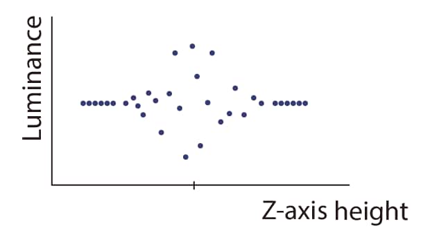
The composite waveform of the interference stripe intensity can be reproduced from the interference fringes captured at regular intervals using an arithmetic formula.
Composite Waveform Representing Interference Stripe Intensity
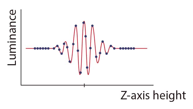
The peak of the created composite waveform is the focal point position of the lens. Height can be determined through synchronization with the travel distance of the lens.
Key Points for White Light Interferometry
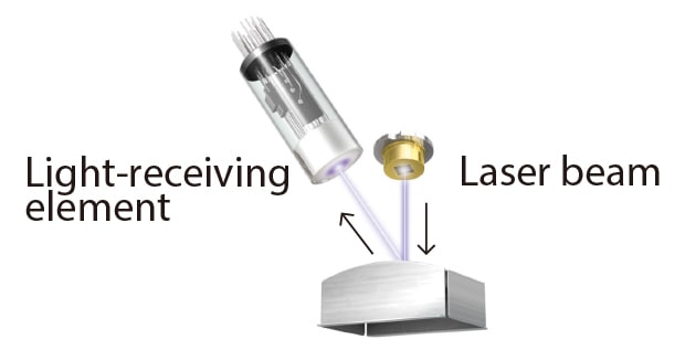
Focusing
With white light interferometers, weak interference signals from low-reflectivity surfaces can make it difficult to achieve accurate focus. The VK-X4000 addresses this challenge with a built-in laser auto-focus function, enabling precise and reliable focusing even on weakly reflective surfaces.
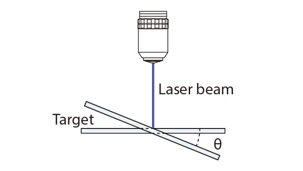
Zeroing
To ensure accurate measurement with a white light interferometer, the target must be leveled, otherwise known as zeroing. With conventional systems, ensuring the target is level required users to check the interference stripes visually and readjust several times. KEYENCE's 3D Optical Profiling Microscope has a built-in zeroing support function to detect any tilting of the target and automatically calculate the correction angle. Being able to determine the correction angle in advance allows for easy, reliable, and fast adjustment.
How White Light Interferometry Works
White light interferometry operates through a process known as vertical scanning. The system moves the objective lens up and down while continuously monitoring interference patterns at each height. White light contains multiple wavelengths, creating a composite interference signal that peaks sharply when the surface is at the focal plane.
Software tracks the vertical position of this intensity peak for every pixel across the entire field of view. A linear encoder measures lens position precisely as it scans, linking each interference maximum to a specific height coordinate. This technique, known as Vertical Scanning Interferometry (VSI), offers a significant advantage over single-wavelength systems, particularly for measuring larger step heights. The distinct, unambiguous nature of the white light interference peak eliminates the ambiguity that can confuse single-wavelength measurements, ensuring reliable data across complex surface features.
Achieving Nanometer-Level Surface Resolution
Resolution comes from mathematical processing rather than optical magnification alone. A 408 nm light source produces fringes spaced 0.204 micrometers apart. Software divides this waveform into thousands of segments, enabling sub-nanometer height discrimination.
This makes white light interferometry valuable for measuring extremely smooth surfaces, such as polished optics, semiconductor wafers, surface coatings and roughness, and film thickness.
Benefits of White Light Interference for Surface Analysis
One of the standout advantages of white light interference is its wide-field measurement capability. Rather than building images point by point like scanning probe methods, white light systems capture entire areas at once, dramatically reducing measurement time.
The technique is also non-contact, meaning delicate samples such as thin films, soft coatings, and cleanroom components can be fully characterized without any risk of contamination or damage. Combined with sub-nanometer vertical resolution, this makes white light interference well-suited for detecting subtle surface features that influence optical performance, friction, and sealing across a wide range of precision manufacturing applications.
White Light Interferometers Characteristics
| Advantages | Disadvantages |
|---|---|
|
Advantages
|
Disadvantages
|
White Light Scanning for 3D Surface Measurement
Modern systems combine white light interference with laser confocal scanning to expand measurement capabilities. Our Optical Profilometer Resources page demonstrates how KEYENCE 3D Optical Profilers use this hybrid approach to adapt to diverse surface characteristics.
The system uses white light scanning for maximum resolution on reflective areas and can switch to confocal methods for steep angles, rough textures, or difficult materials. This allows users to measure complex samples in a single session without needing multiple instruments. Additionally, the high-resolution objective lenses can produce stunning, true-color images of a surface.
Applications of White Light Interferometers
White light interferometers are used across industries where surface geometry must be measured at the nanometer to micrometer scale without contact.
Semiconductor manufacturing is one of the most demanding application areas. Wafer step height verification, film thickness measurement, and substrate flatness all require sub-nanometer precision, since defects at that scale directly impact device yield. As feature sizes continue to shrink, interferometry has become a standard process control tool at multiple stages of fabrication.
Optics manufacturers rely on these systems to verify lens curvature, mirror flatness, and the uniformity of optical coatings since any surface deviation introduces aberration that degrades optical performance. Similarly, precision machined components such as cutting tools, bearing surfaces, and mold cavities are measured to confirm surface finish and dimensional tolerances that contact-based profilometers cannot reach without risking part damage.
In materials research and failure analysis, interferometry is used to characterize wear patterns, corrosion, fracture surfaces, and thin film behavior. Because measurements are non-destructive, the same sample can be measured repeatedly across test intervals to track how a surface evolves over time.
Medical device manufacturing represents a growing application area, where surface texture of implants and the geometry of micro-machined components must meet tight regulatory and functional tolerances. Data storage component inspection, such as read/write head flatness and disk surface quality, has historically been another high-precision use case driven by the same need for nanoscale surface control.
3D Optical Profiling Microscopes Overcome Limitations of White Light Interferometers
Solutions for Low Angular Characteristics
| Difficulties with interferometers | Solved with KEYENCE's 3D Optical Profiling Microscope |
|---|---|
|
Difficulties with interferometers
Interferometers can struggle to accurately measure objects with steep surface angles. In these areas, interference fringes become highly concentrated, making it difficult to capture reliable data. |
Solved with Keyence's 3D Surface Profiler
The laser scanning confocal method of the VK-X Series is able to accurately measure surfaces with angles approaching 90 degrees. |
Observation with Interferometer
Curved surfaces cannot be measured due to tightly packed interference fringes.
Observation with 3D Optical Profiling Microscope
Short wavelength laser confocal systems can detect very faint reflections and don’t rely on fringe patterns.
Solutions for Material Limitations
| Difficulties with interferometers | Solved with KEYENCE's 3D Optical Profiling Microscope |
|---|---|
|
Difficulties with interferometers
White light interferometry works by combining reflected light from the sample surface with light from an internal reference mirror to create interference patterns. This means the technique works best on smooth, mirror-like surfaces and struggles in a few key situations. |
Solved with Keyence's 3D Surface Profiler
By integrating three different measurement principles, the VK-X Series 3D Optical Profiling Microscope can choose a technique that’s optimized for the material being measured. In cases where white light interferometry struggles due to material or surface topography, laser scanning may be a better alternative. Because laser scanning microscopes use a photomultiplier (PMT) with a wide sensitivity range, surfaces that include areas of both high and low reflectivity can be measured accurately, including those with steep slopes. |
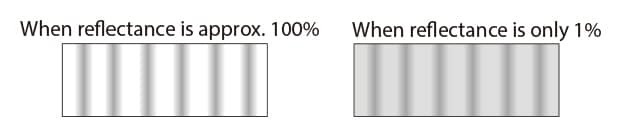
If the reflectance from the reference surface is 100% and the reflectance from the measurement surface is also approximately 100%, clear interference stripes appear.
However, if the reflectance from the measurement surface is only 1%, the contrast is not as defined.
Solutions for Slope Correction
| Difficulties with interferometers | Solved with KEYENCE's 3D Optical Profiling Microscope |
|---|---|
|
Difficulties with interferometers
Before measurement, slope correction of the sample with a goniometer stage is required. |
Solved with Keyence's 3D Surface Profiler
KEYENCE's 3D Optical Profiling Microscope is equipped with both white light interferometry and laser confocal scanning, so that nearly any sample can be measured, including those with steep angles. |
Solutions for Low Lateral Resolution
| Difficulties with interferometers | Solved with KEYENCE's 3D Optical Profiling Microscope |
|---|---|
|
Difficulties with interferometers
Since interferometers operate on white light, the lateral resolution of these systems will be the same as a conventional optical microscope - approximately 0.43 μm (0.017 mil). |
Solved with Keyence's 3D Surface Profiler
By using a short wavelength laser in a confocal configuration, users can achieve a lateral resolution of 0.13 μm (0.005 mil). |

Frequently Asked Questions
What Is a White Light Interferometer Used For?
It measures surface topography with sub-nanometer precision on smooth, reflective samples. Key uses include semiconductor step height verification, film thickness measurement, and optical quality assessment.
How Does White Light Interferometry Work?
A beam splitter divides light into reference and measurement paths. When recombined, they create interference patterns. As the lens scans vertically, software analyzes these patterns to calculate the height of every point on the surface.
What Are the Advantages of White Light Interference Measurement?
- Precision: Sub-nanometer vertical resolution.
- Efficiency: Fast, wide-field-of-view data capture.
- Safety: Non-contact operation that protects delicate surfaces.
- Superiority: Excels on smooth surfaces where other methods fail.
How Accurate are White Light Interferometers for Surface Profiling?
Vertical resolution can reach angstrom levels. While highly accurate on flat, reflective materials, performance may decrease on steep slopes or low-reflectivity surfaces.