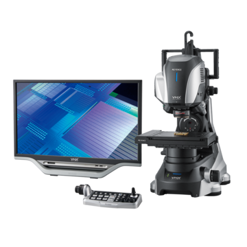
Digital Microscopes
Observation and Measurement of Printed Boards
Smartphones, tablets, wearable devices, and other similar devices have been designed to be smaller, thinner, and with higher functionality. Because of this, PCBs and components have also been designed to be smaller, denser, and with more layers.
Consequently, it has become more difficult to observe fine parts (such as through holes, lands, and pads) and measure 3D shapes (such as surface irregularities) for the research and development and quality assurance of printed circuit boards (PCBs) and printed wired boards (PWBs). This section introduces the basic knowledge of PWBs and PCB mounting as well as observation and measurement examples using our digital microscope.
Types, Structures, and Characteristics of PWBs
In PCB manufacturing, quality after component mounting depends on PWBs.
Types of PWBs
The PWB types, characteristics, and structures are explained below with figures.
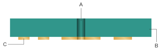
A: Non-plated through hole B: Substrate C: Copper foil
Single-sided board (one layer board)
Only one side of the substrate is printed with copper foil. Having only one layer, it is called a single layer board. Non-plated through holes, into which component leads or electrodes are inserted, are drilled or punched on the substrate and the insides of these holes are insulated because they are not plated with copper. Lands or pads on the substrate surface are covered with copper foil to be contacted with the components that will be mounted. Single-sided boards are often used for mass-produced electronics for consumer use because of low manufacturing costs.
A: Through hole B: Substrate C: Copper foil
Double-sided board (two-layer board)
Both sides of the substrate are printed with copper foil. This type is called a two layer board. The insides of the through holes used for mounting components are conductive because they are plated with copper. The manufacturing costs are higher than those of single-sided boards. Yet, this type is widely used for electronics because the area for wiring and mounting is twice as large as single-sided boards, reducing the size of the substrate to use.
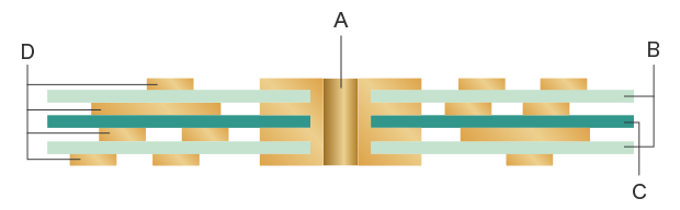
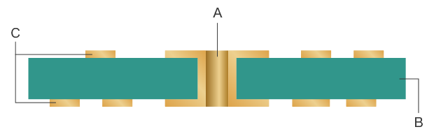
A: Through hole B: Prepreg (insulating layers) C: Substrate D: Copper foil
Multi-layer board
Multi-layer boards laminate copper foil and insulating layers called prepreg. This type is called a four-layer board, six-layer board, or eight-layer board according to the number of laminated layers. The more layers a board has, the more complex its structure. The designing and manufacturing costs increase accordingly. At the same time, multi-layer boards can contain power circuits and general signal lines between layers, increasing the surface area used for mounting and also increasing the mounting density.
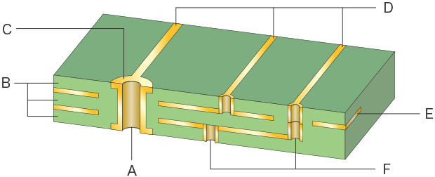
A: Through hole B: Prepreg (insulating layers) C: Land (pad) D: Tracks (patterns) E: Plane layer or wire layer F: Vias
Names of PWB parts
In a multi-layer board, holes that connect different circuit layers are called vias (F in the figure below). A part around a through hole on the substrate surface, called a land or pad, is used to solder leads of electronic components (C in the figure below).
Get detailed information on our products by downloading our catalog.
View Catalog

PCB Mounting Methods
PCB mounting is a process to solder electronic components on a PWB to function as a PCB. Two methods are commonly used to mount electronic components on PWBs: insertion mount technology and surface-mount technology. The characteristics of each technology are introduced below with figures.
Insertion mount technology (IMT)
This technology solders leads or electrodes inserted into through holes on a PWB. Solder applied to the inside of the through hole slightly reduces the impedance at the joint. A disadvantage of this technology is that components arranged on the surface require a larger substrate, making it difficult to miniaturize the PCB.
The leads on the components to mount are straight and point down for insertion into through holes. These components are called dual in-line packages (DIPs).
A component is connected by inserting the leads into through holes.
DIPs
Surface mount technology (SMT)
Surface mount technology (SMT) is now most commonly used for PCB mounting. Electronic components are mounted on solder and applied to lands on the PWB and bonded by heating in a furnace, through holes are not used, in a process called reflow soldering. Unlike IMT, leads or electrodes do not need to pass through PWBs, so SMT can arrange components on both sides of a PWB efficiently with high flexibility. SMT can mount a larger number of electronic components, making PCBs smaller and denser.
Components to mount on surfaces, which are called surface mount devices (SMDs), are packages having lead tips parallel to lands or have electrodes at both bottom edges or on their sides.
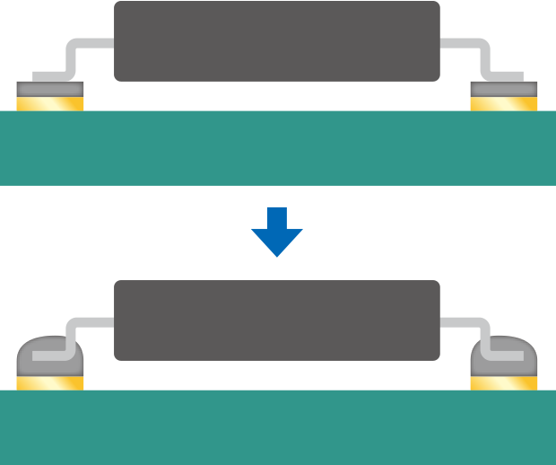
Leads or electrodes are placed on lands and bonded.
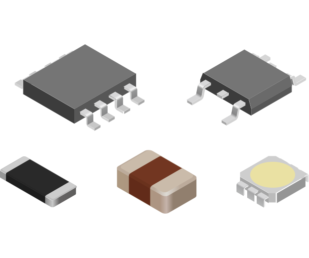
SMDs

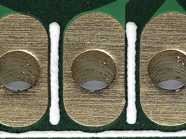
Observation and Measurement Examples of Through Holes and Lands on PWBs
Through holes and lands on PWBs play an important role in connecting components to PWBs and other components in circuits. In the mounting process, various items need to be controlled, such as solder printing, solder bath conditions, and temperature profiles of reflow furnaces. Even with the most careful attention to each process and material, defective through holes and lands can cause PCB conduction failures or malfunctions.
Through holes and lands on PWBs have surface irregularities and reflection specific to copper foil. It is difficult to observe PWBs at an angle with conventional microscopes partly because it takes a lot of time and effort and only a part of the surface irregularities can be brought into focus. It is also difficult to measure 3D shapes and dimensions of microscopic through holes and lands on very small PWBs.
KEYENCE's VHX Series digital microscope is equipped with advanced imaging capabilities and various functions that help users easily capture high-resolution images and accurate measurements, improving the research and development and quality assurance of PCBs and PWBs.
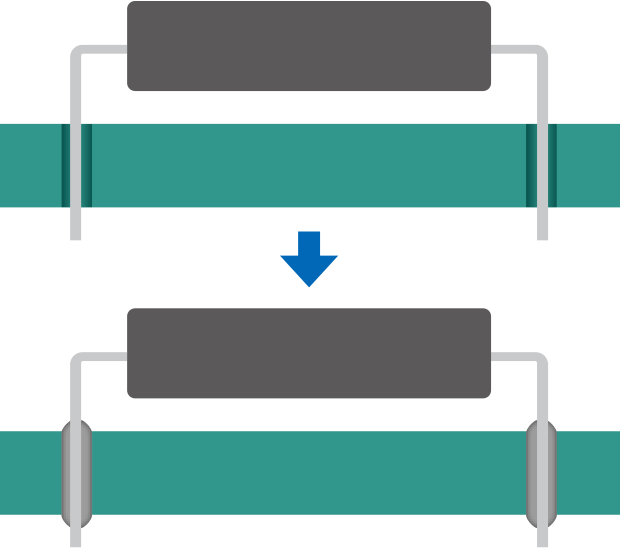
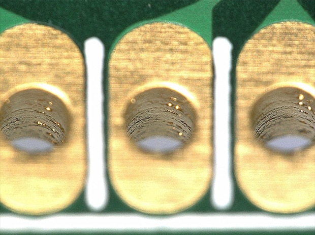
Tilted observation of through holes
Copper plating peeled from the inside of through holes can cause contact failures. To observe deep holes with a conventional microscope, it is necessary to repeat tilted observation on a sample fixed at an angle with a jig, which is difficult and takes a lot of time and effort.
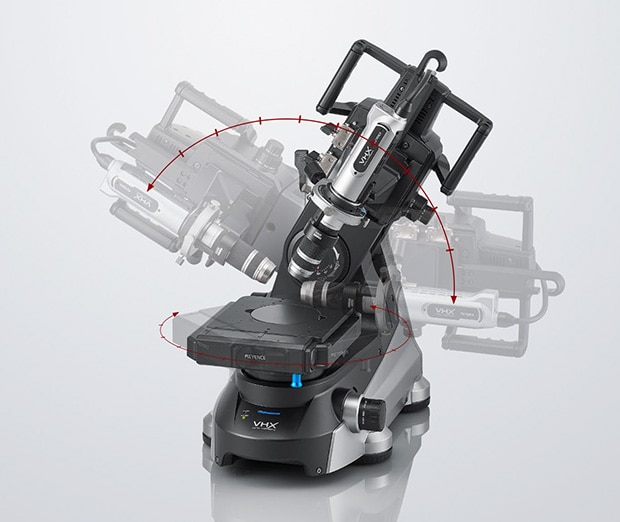
The VHX Series digital microscope combines a free-angle observation system with a motorized XYZ stage so the target stays centered in the field of view even if the lens is tilted or rotated.
Additionally, the depth composition function allows users to capture fully-focused images, like the inside of through holes, from any angle or magnification.
Tilted observation of through holes using the VHX Series 4K digital microscope
The VHX Series can also automatically determine the optimum lighting conditions using the Multi-lighting function, which obtains images captured with omnidirectional lighting.
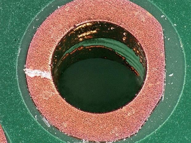
The following image shows the inside of a through hole using tilted observation, which is difficult to illuminate, using a combination of ring illumination and backlighting. Even microscopic defects such as copper foil peeled from the hole surface can be closely observed.
Ring illumination (100x)

Ring illumination + depth composition (100x)
Ring illumination (150x)
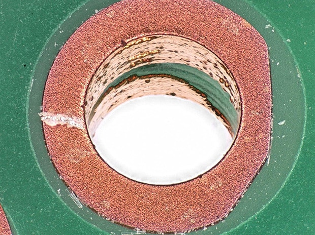
Ring illumination + backlighting (150x)
Observation of surface irregularities on lands
There are subtle surface irregularities on copper-plated land surfaces that are difficult to capture due to low contrast.
The VHX Series digital microscope is equipped with Optical Shadow Effect Mode, which easily captures high-contrast images that rival a scanning electron microscope (SEM), while eliminating the need for preparation such as vacuuming. The surface conditions can be closely observed and evaluated using an image emphasizing the surface irregularities.
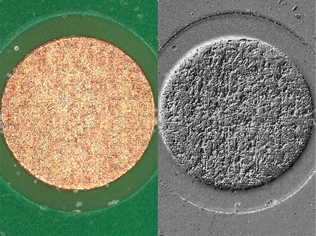
Left: Ring illumination (150x)/Right: Optical Shadow Effect Mode image (150x)
Optical Shadow Effect Mode image showing the surface conditions of a land captured using the VHX Series 4K digital microscope
3D measurement and profile measurement of defective plating on lands
Defective lands on PWBs can cause PCB malfunctions or problems in the component mounting process and are difficult to measure using contact measuring instruments or conventional microscopes.
The VHX Series digital microscope can quickly capture accurate 3D measurements at sub-micron levels of uneven shapes, subtle surface irregularities and roughness just by clicking at the specified locations on the image.
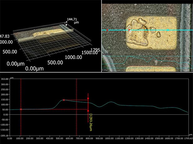
Ring illumination + HDR image (200x)/3D measurement and profile measurement
3D measurement of defects on a land using the VHX Series 4K digital microscope
A Digital Microscope that Enhances Research and Development and the Quality Assurance of PWBs and PCBs
The VHX Series digital microscope allows any user to quickly capture high-resolution images and accurate measurement of through holes and lands on PWBs that are essential in improving the PCB reliability. All the images and data can be automatically exported to a report, reducing the amount of time it takes for analysis.
The VHX Series is equipped with many other functions not introduced here. For additional product info or inquiries, click the buttons below.
Get detailed information on our products by downloading our catalog.
View Catalog