Digital Microscopes
PCB Failure Analysis and PCB Defect Analysis
Smartphones and other devices increasingly require smaller and denser PCBs and electronic components. In the automotive industry, automatic brake and autonomous driving technologies have promoted computerized control. There is increasing demand for reliable PCBs and quality improvement through failure and defect analysis.
This section introduces new examples of PCB failure analysis and PCB defect analysis using KEYENCE's latest 4K Digital Microscope.
Importance of PCB Failure Analysis
As smartphones, tablets, and wearable devices have become smaller, thinner, and more functional, PCBs and components continue to be even smaller, denser, and more layered. In the automotive industry, research and development of technologies such as automatic brakes and autonomous driving has promoted computerized control of important components. Such control then expects PCBs and electronic components to have high durability and reliability so as to withstand long-term stress caused by driving, accelerating, and stopping.
Terminals and devices now have an important role in various daily situations, and cars require a high degree of safety. Any failures and defects of important components that are computerized in such products can lead to serious trouble or accidents.
To evaluate the durability and reliability of PCBs and electronic components, reliability evaluation tests, including acceleration tests, have become increasingly important. In addition to such tests, using microscopes to identify defects and failure causes is more important than ever.
This section explains methods of PCB defect analysis and PCB failure analysis for failures caused during manufacturing and shipping.
Get detailed information on our products by downloading our catalog.
View Catalog

Methods of PCB Failure Analysis and PCB Defect Analysis
The following methods are used in identifying PCB defects and failures:
- Identifying failure locations
Failure locations are identified through a variety of devices and techniques, including spectroscopy, microtomography, and micro thermography. - Understanding failure locations
To correctly understand the physical properties of microscopic structures, they are observed using a transmission X-ray microscope, CT scanner, electron probe micro analyzer (EPMA), or other instruments. - Observing and analyzing defective areas
To identify specific causes, defects are closely analyzed through cross-section observation of defective areas, which uses tools such as microscopes, scanning electron microscopes (SEMs), focused ion beam (FIB) microscopes, and EPMAs.

Latest Examples of Observation and Analysis of PCBs
In the PCB failure analysis and PCB defect analysis introduced in the previous section, the accuracy of the observation and analysis of defective areas is particularly important. To identify causes of failures, analysis and evaluation need to be fast and accurate.
Microscopes are often used to inspect the appearances of defective areas in such analysis and evaluation. Conventional procedures, however, tend to be complicated due to using large systems or combining multiple systems, and thus take a long time to complete. The procedures also have many problems in terms of observation and analysis due to uneven surfaces of tiny parts, indeterminable lighting conditions, and subtle contours.
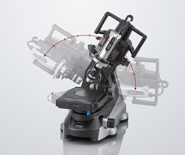
KEYENCE's VHX Series high-definition 4K Digital Microscope uses a high-resolution HR lens and cutting-edge technology, such as a 4K CMOS image sensor, enabling accurate observation and analysis of defective areas with clear 4K images. The VHX Series also supports 2D and 3D measurements with easy operation, enabling quick completion of all required analysis tasks.
This section introduces the latest examples of observation and analysis using the VHX Series.
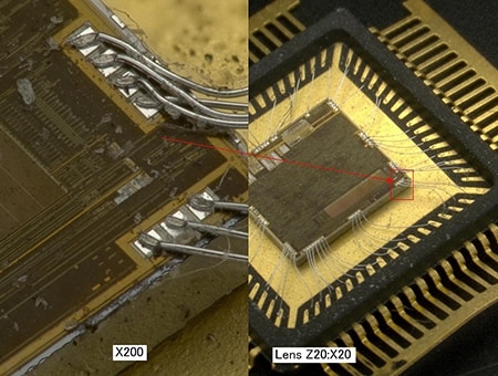
Observation and analysis of wire bonding
Conventional systems only focus on part of the three-dimensional wire bonding connected to a die and are also affected by glare from reflective surfaces. These issues make it extremely difficult to capture clear images.
The VHX Series 4K Digital Microscope has a free-angle observation system, which enables tilted observation from any angle; uniform lighting, which is achieved with the highly functional built-in light; a glare removal function, which reduces glare from reflective surfaces; and real-time depth composition, which brings the entire three-dimensional target into focus. These features allow users to observe and analyze wire bonding with clear, fully-focused images.
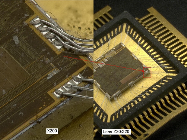
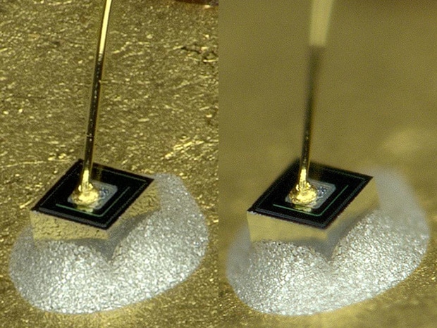
Tilted observation and analysis of wire bonding using the VHX Series 4K Digital Microscope
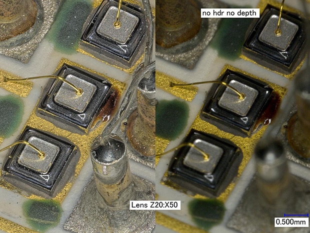
Left: HDR imaging + depth composition/right: normal (50x)
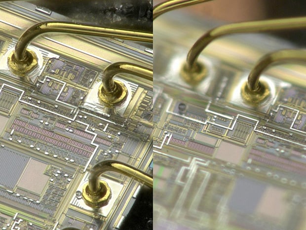
Left: depth composition/right: normal (200x)
Split-screen display of high-/low-magnification observation(left: 200x/right: 20x)
Left: depth composition/right: normal
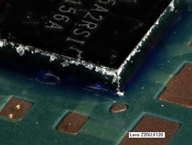
Observation and analysis of cross sections and surfaces of semiconductor packages
The VHX Series 4K Digital Microscope is equipped with versatile lighting, including darkfield, brightfield, differential interference contrast (DIC), and polarized lighting. This versatile lighting allows users to observe the characteristics of glues and pastes that are used for semiconductor packaging.
Even if the cross section of a resin-embedded sample has irregularities due to cutting or polishing, the surface can still be accurately observed.
Observation and analysis of cross sections of a resin-embedded BGA using the VHX Series 4K Digital Microscope
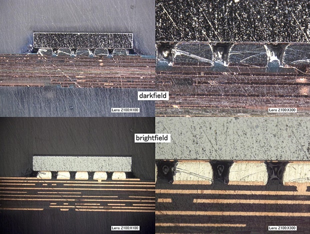
Top: darkfield lighting (100x and 300x)/bottom: brightfield lighting (100x and 300x)
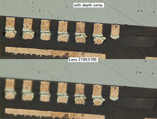
Top: depth composition/bottom: normal (700x)
With the free-angle observation system of the VHX Series, package surfaces and pins can be observed at high magnification from any angle. A depth of field that is approximately 20 times deeper than that of conventional microscopes enables quick and highly accurate analysis with fully focused images, eliminating the need for troublesome adjustments.
Tilted observation of a semiconductor package using the VHX Series 4K Digital Microscope
Tilted observation of a package surface (120x)
Tilted observation of leads (split-screen function)
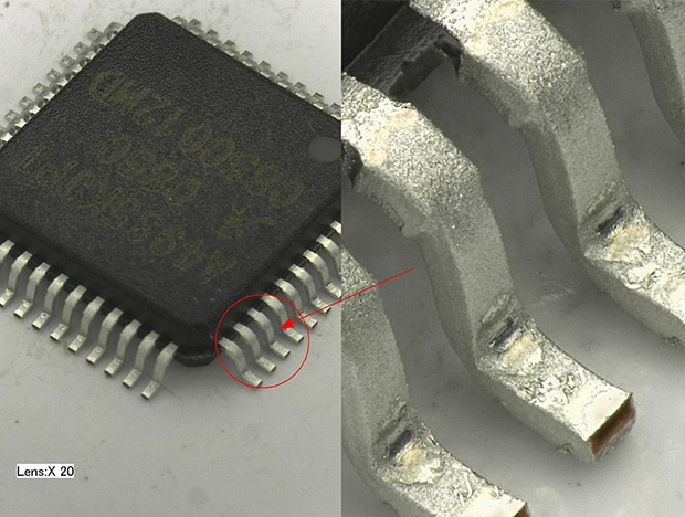
Observation, measurement, and analysis of PCBs
Printed circuit boards (PCBs)—on which electronic components are mounted—have irregularities, various colors, and reflectivity on their surfaces. These issues have conventionally made it difficult to determine the focusing and lighting conditions, leading to such work taking a long time to complete.
The high-resolution HR lens and motorized revolver of the VHX Series 4K Digital Microscope enable a seamless zoom function that automatically switches between lenses from 20x to 6000x magnification. This function allows users to perform zooming and observation with intuitive operations. With the free-angle observation system, fully focused, high-resolution images can be captured even in tilted observation at high magnification. Therefore, three-dimensional mounting components can be observed and analyzed clearly. Images at different magnifications can be displayed side by side using the split-screen function, allowing users to always track the defective mounting area to analyze, even in the case of dense PCBs.
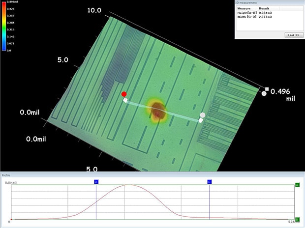
Furthermore, 3D shape and profile measurements can be performed directly on a high-resolution image using the height information, allowing users to complete quantitative analysis and evaluation with a single unit.
Observation, analysis, and measurement of component mounting conditions using the VHX Series 4K Digital Microscope
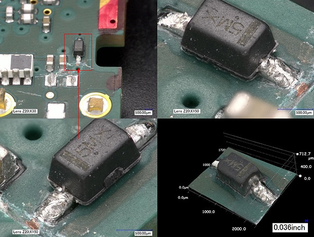
Tilted observation and 3D shape measurement (split-screen function)
The profile of the desired cross section can be measured.
Final appearance inspection of IC chips
The VHX Series 4K Digital Microscope supports high magnifications up to 6000x, thereby enabling the capturing of high-resolution 4K images even at high magnification. With depth composition and the HDR function, targets having irregular surfaces can be fully focused under various lighting conditions, thereby allowing users to capture even subtle scratches on IC chip patterns.
In addition to PCB failure analysis and PCB defect analysis, quick and accurate analyses and evaluations can be performed in the final appearance inspections carried out at manufacturing sites.
Appearance inspection of IC chips using the VHX Series 4K Digital Microscope
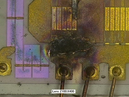
Left: brightfield lighting/right: darkfield lighting (400x)
Differential interference contrast (DIC) lighting
High-resolution imaging of IC patterns under blue light
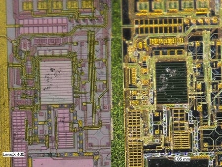
Failure analysis and defect analysis of an IC chip using the VHX Series 4K Digital Microscope
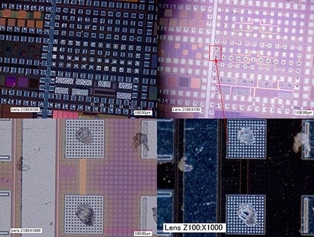
Low-magnification and high-magnification analysis images of a failure location (up to 1000x)
Analysis of a defective area (400x)
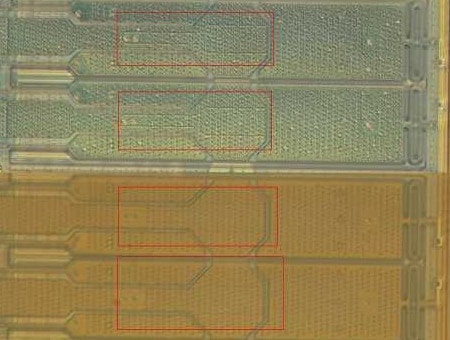
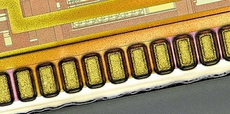
Inspection and analysis of foreign particles mixed into IC chips
Foreign particles mixed in circuits can cause short-circuits, resulting in component failures and defects.
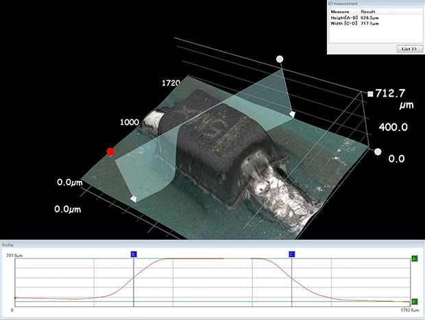
The VHX Series 4K Digital Microscope captures clear images of foreign particles at high magnification. 3D imaging allows users to separate foreign particles from irregularities on the circuit surface.
Furthermore, the VHX Series enables 3D shape and profile measurements of foreign particles using the height information from 3D imaging. A single unit makes it possible to identify foreign particles, evaluate their size, and create a report, greatly increasing throughput.
Analysis of a foreign particle mixed into an IC chip using the VHX Series 4K Digital Microscope
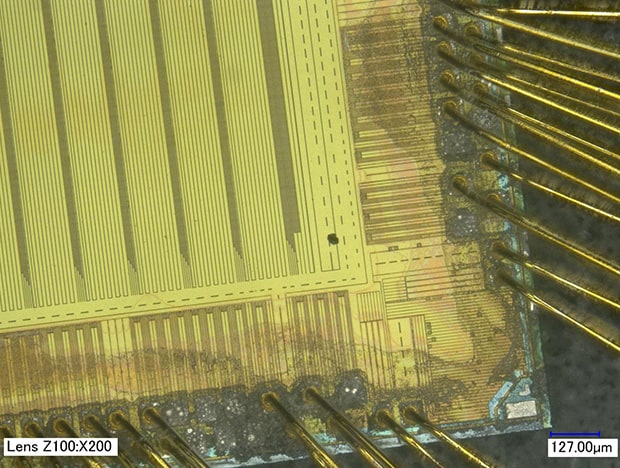
Area having a foreign particle on an IC chip (200x)
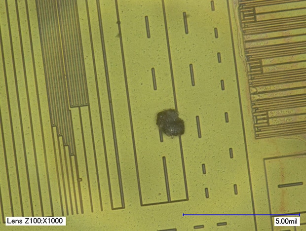
Foreign particle mixed into an IC chip (1000x)
Profile measurement of a foreign particle
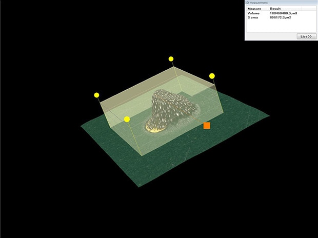
3D shape measurement of a foreign particle
Improved Accuracy and Work Efficiency of PCB Failure Analysis and PCB Defect Analysis
The VHX Series 4K Digital Microscope enables fast observation and imaging as well as 2D and 3D measurements. With all of these features combined into one unit, PCB defect and failure analysis is faster and more efficient.
Advanced analysis and quantitative evaluation can be performed with simple operations, allowing anyone, regardless of skill level, to obtain the same results.
In addition to the functions introduced here, the VHX Series is equipped with many more functions, supporting analysis of various failures and defects that occur in various types of targets.
For additional product info or inquiries, click the buttons below.
Get detailed information on our products by downloading our catalog.
View Catalog