3D Optical Profilometers
What Is an Optical Profilometer?
Key Takeaways
- Optical profilometers provide precise, non-contact 3D surface measurement to capture data at the micro- and nanoscale, ensuring accurate results without damaging delicate materials.
- Different optical techniques like white light interferometry, confocal microscopy, structured illumination, and focus variation handle everything from smooth reflective surfaces to rough or transparent materials.
- Non-contact measurement enhances precision, speed, and durability to capture complete 3D surface maps in seconds with sub-nanometer precision. Non-contact means no wear, drift, or downtime which is ideal for automated inspection.
- From semiconductors and optics to medical devices and 3D printing, optical profilometers analyze roughness, step height, film thickness, and defects all in one scan.
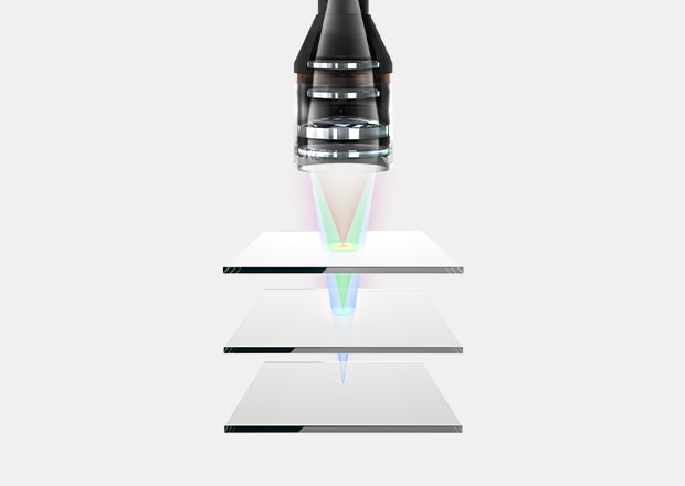
An optical profilometer is a high-precision, non-contact surface metrology tool used to measure the roughness, texture, and topography of surfaces—typically at the micro- and nanoscale. Unlike traditional contact profilometers, which rely on a stylus physically touching the sample, optical profilometers use light-based techniques such as white light interferometry, structured lighting, or confocal microscopy to generate detailed 3D surface data without any physical contact. This makes them ideal for analyzing delicate, soft, or deformable materials, or when higher throughput is needed.
How Does an Optical Profilometer Work?
At its core, an optical profilometer projects light onto a surface and analyzes the interference patterns or focus variations to construct a precise 3D map of the surface. Depending on the specific technology used, it may employ any of these commonly used measurement methods:
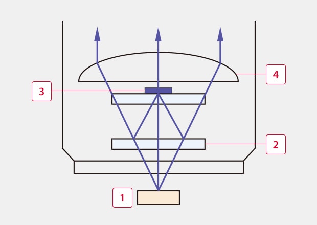
White Light Interferometry (WLI)
WLI uses broad-spectrum white light to generate interference patterns between light reflected from a reference mirror and the surface being measured.
-
1Target
-
2Beam splitter
-
3Reference mirror
-
4Objective lens
Phase-Shifting Interferometry (PSI)
A more precise variant of interferometry where the phase of the light wave is shifted in controlled steps to enhance resolution. It measures extremely smooth surfaces with sub-angstrom accuracy.
Confocal Microscopy (Confocal Profilometry)
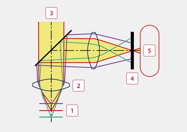
Confocal schematic
Confocal profilometers focus a light beam or laser onto a small point on the surface. The system measures the intensity of reflected light at different focal depths to construct a 3D surface profile.
-
1Focal position
-
2Objective lens
-
3Laser light
-
4Confocal pinhole
-
5Light receiving element
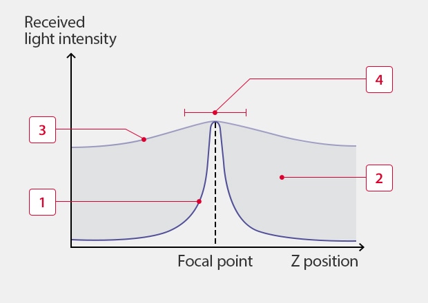
Pinhole confocal principle
Detection of the peak (focal point) by means of the pinhole confocal optical system in comparison to systems without a pinhole.
-
1Z-I curve of the pinhole confocal optical system
-
2Ambient light from points other than the peak (focal point)
-
3Z-I curve (light intensity) of systems without PMT and pinhole
-
4The peak light intensity is broader in conventional optical systems because there is no pinhole
Focus Variation
Focus variation combines optical contrast and vertical scanning to determine surface height. It identifies the position where the image is most sharply focused at each pixel to reconstruct a 3D profile.
Structured Light Projection
A pattern of light (usually stripes or grids) is projected onto the surface, and deformation of the pattern is used to calculate surface height via triangulation.
Chromatic Confocal (Chromatic Dispersion)
Uses a chromatically dispersed white light beam that focuses different wavelengths at different heights. The system detects which wavelength is in focus at a given point to determine surface height.
All these methods allow for non-destructive, high-speed scanning of surfaces with incredibly high precision, but each one will have their own unique advantages when it comes to resolution, speed, and material-type that can be measured.
The table below summarizes some of the general characteristics of these 3D metrology systems:
Summary Comparison Table
| Measuring Principle | Vertical Resolution | Lateral Resolution | Best For |
|---|---|---|---|
|
Measuring principle
White light interferometry (WLI)
|
Vertical resolution
Very high
|
Lateral resolution
High
|
Best for
Flat, smooth, reflective surfaces
|
|
Measuring principle
Phase-shifting interferometry (PSI)
|
Vertical resolution
Ultra-high
|
Lateral resolution
High
|
Best for
Atomically smooth surfaces
|
|
Measuring principle
Confocal microscopy
|
Vertical resolution
High
|
Lateral resolution
Very high
|
Best for
Steep slopes, rough or textured surfaces
|
|
Measuring principle
Focus variation
|
Vertical resolution
High
|
Lateral resolution
High
|
Best for
Larger heights, high-slope surfaces
|
|
Measuring principle
Structured light projection
|
Vertical resolution
Moderate-high
|
Lateral resolution
Moderate
|
Best for
Large, general-purpose surface inspections
|
|
Measuring principle
Chromatic confocal
|
Vertical resolution
High
|
Lateral resolution
Moderate–high
|
Best for
Transparent or multi-material surfaces
|
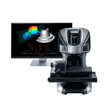
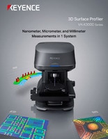
At KEYENCE, we have two systems that function as optical profilometers—each incorporating their own scanning methods to suit your application needs. These methods include focus variation, confocal microscopy, white light interferometry, and structured light projection, with the first three options all integrated within a single system. Check out our VR-6000 Series Wide-Area Optical Profiler by downloading the catalog below.
Get detailed information on our products by downloading our catalog.
View Catalog

Key Advantages of Optical Profilometry
Optical profilometry has become a preferred choice in surface characterization because it overcomes many of the limitations of traditional contact-based methods. Perhaps its most significant advantage is that it is entirely non-contact. By relying on light rather than a stylus, the technique avoids damaging delicate samples. This makes it particularly valuable in fields like semiconductor manufacturing, medical devices, and optics, where even the smallest scratch or surface disturbance can compromise performance. Beyond protecting fragile materials, optical systems also make it possible to measure samples that were once considered unmeasurable, including soft, viscous, or adhesive materials, with accuracy and confidence.
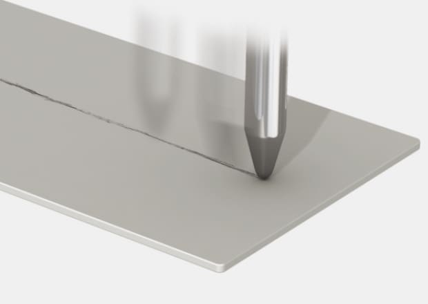
The sample is scratched.
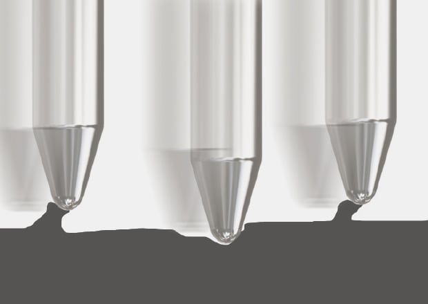
Soft or adhesive samples are difficult to measure.
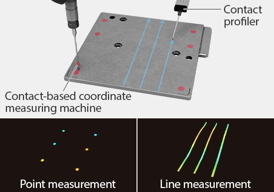
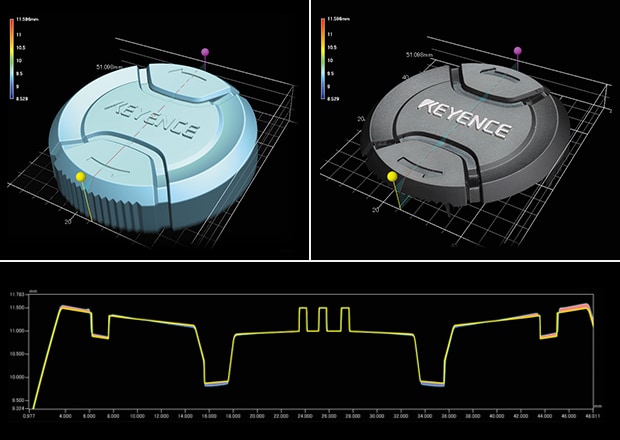
In terms of resolution, 3D optical profilers deliver exceptional precision. Many systems are capable of sub-nanometer vertical resolution, revealing height variations far too subtle for a stylus to detect, while still offering micron-scale lateral detail. Unlike contact profilometers that record surface topography line by line, optical profilometers can capture full three-dimensional maps of a surface area in seconds. This not only accelerates inspection but also provides a more comprehensive view of surface geometry, enabling analysis of roughness, step height, volume, and flatness all from a single scan.
Conventional Measurement Instruments
Some shapes cannot be analyzed with conventional measurement methods.
Wide-Area Optical Profiler
Measuring the entire surface reveals the true shape.
Another key strength is versatility. Optical profilometers can be used across a wide range of materials and finishes, from reflective metals and glass to polymers and rough coatings. They handle both highly polished and irregular surfaces with equal effectiveness, with laser-based systems being the preferred method for more difficult material types. Because there is no physical tip making contact, there is also no risk of tool wear or calibration drift, which means results remain consistent over time and maintenance requirements are minimized.
The wealth of data these systems provide, combined with their speed and reliability, makes them especially suited for automated inspection environments. In high-throughput production, the ability to measure quickly, accurately, and without contact allows manufacturers to maintain tight quality standards without slowing down operations.
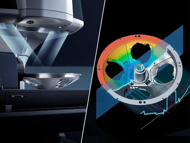
KEYENCE’s optical profilers are designed to handle the widest range of surface measurement needs—from detecting sub-nanometer variations to accurately analyzing complex, highly irregular surfaces that conventional white light interferometers often cannot measure. Because the system is completely non-contact, it excels in situations where a probe or stylus cannot physically reach. In addition, KEYENCE profilers capture data across a larger area in a single scan, giving users a faster, more comprehensive view of surface characteristics.

Common Applications of Optical Profilometers
Optical profilometers are widely used across industries where surface quality and precision manufacturing are critical. Some common applications and uses include:
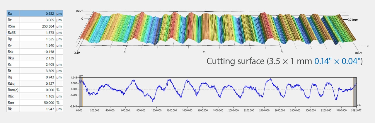
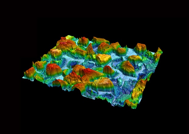
Surface Roughness and Texture Analysis
- What it is:
- Measuring micro- and nano-scale surface variations to quantify how smooth or rough a material is.
- Why it matters:
- Roughness affects friction, wear, adhesion, coating performance, and even optical reflectivity.
- Typical industries:
- Precision machining, automotive, aerospace, medical implants, optics.
Step gauge (8 nm) (200×)
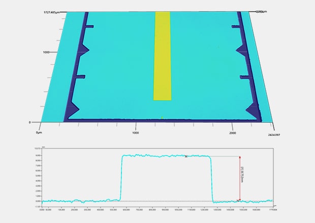
Step Height Measurement
- What it is:
- Measuring the vertical difference between two surface regions, such as thin films, etched patterns, or layered coatings.
- Why it matters:
- Essential for semiconductor wafers, MEMS devices, and multilayer coatings where layer thickness must be tightly controlled.
- Advantage:
- Optical systems can resolve step heights down to the nanometer scale, far beyond most mechanical methods.
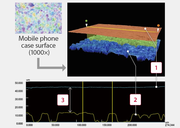
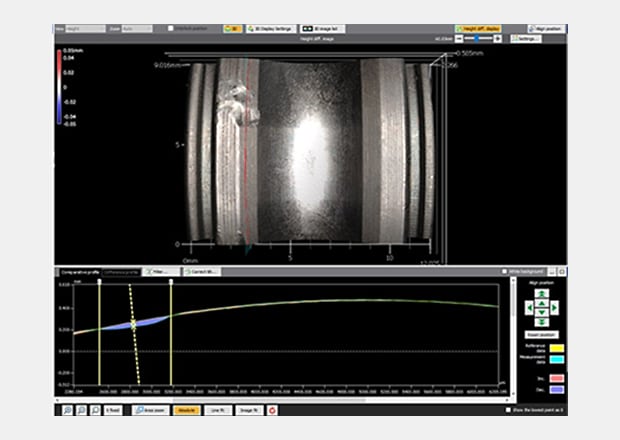
Thin Film Thickness Measurement
- What it is:
- Determining the thickness of transparent or semi-transparent films.
- Why it matters:
- Thin films are ubiquitous in electronics, optics, and solar cells; thickness directly impacts performance.
- Typical industries:
- Semiconductor, photovoltaics, display technology.
-
1Clear coated surface
-
2Plastic case surface
-
3Thickness of clear coating
Flatness and Form Evaluation
- What it is:
- Assessing deviations from an ideal flat or curved surface.
- Why it matters:
- Optical components, sealing surfaces, and high-precision machined parts must meet strict flatness tolerances to function properly.
- Example:
- Ensuring lenses, mirrors, or sealing flanges meet precise specifications.
Defect and Wear Analysis
- What it is:
- Detecting scratches, pits, cracks, or wear patterns on surfaces.
- Why it matters:
- Even microscopic defects can lead to part failure or reduced efficiency, especially in high-performance systems (ball bearings, joint implants, etc.).
- Advantage:
- 3D surface maps provide quantitative defect analysis rather than just visual inspection.
Diamond tool (400×)
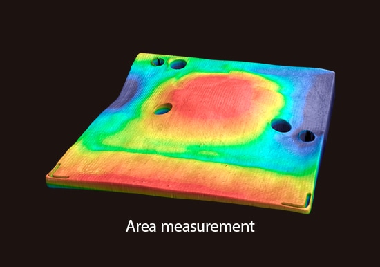
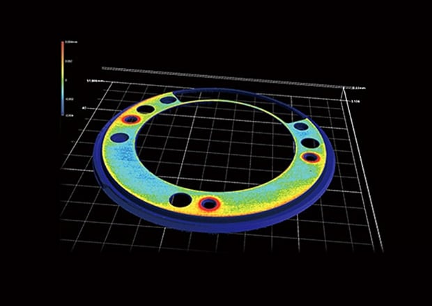
3D Surface Topography and Mapping
- What it is:
- Capturing a complete 3D representation of a surface rather than just a single profile line.
- Why it matters:
- Provides richer data for R&D, quality control, and functional surface analysis (e.g., tribology, fluid retention, optical scattering).
- Applications:
- Aerospace turbine blades, medical stents, optical lens molds.
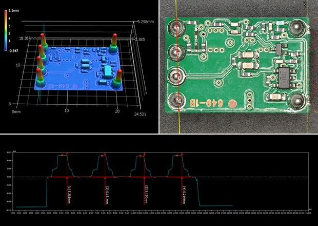
Microelectronics and Semiconductor Metrology
- What it is:
- Measuring wafers, microcircuits, MEMS structures, and microfabricated features.
- Why it matters:
- In semiconductor production, nanometer-scale accuracy is critical; non-contact methods ensure surfaces aren’t contaminated or damaged.
- Advantage:
- Optical profilometers can handle both smooth wafer surfaces and structured patterns.
Additive Manufacturing (3D Printing)
- What it is:
- Inspecting layer-by-layer surfaces and final printed components.
- Why it matters:
- Surface quality directly affects part strength, fatigue resistance, and function.
- Advantage:
- Optical methods quickly verify roughness, layer thickness, and uniformity without damaging prototypes or parts.
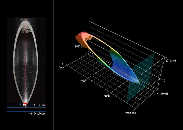
Hypodermic needle
Biomedical and Implant Surface Characterization
- What it is:
- Measuring surface features of implants, stents, and prosthetics.
- Why it matters:
- Surface roughness and texture affect how implants integrate with biological tissue (osseointegration, cell adhesion).
- Advantage:
- Non-destructive inspection ensures medical devices remain sterile and undamaged.
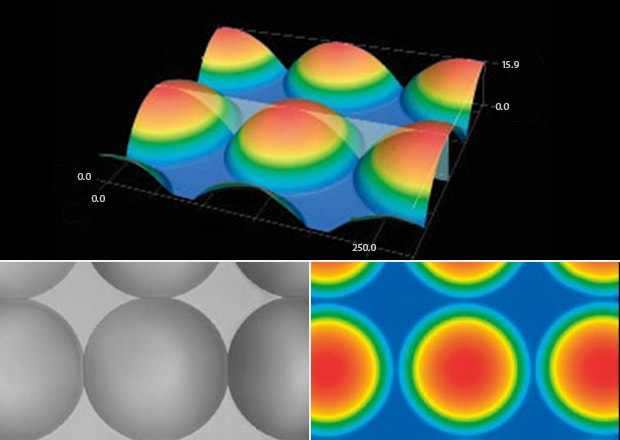
Microlens array
Optical Component Inspection
- What it is:
- Ensuring lenses, mirrors, and coatings meet surface form and roughness requirements.
- Why it matters:
- Even tiny surface defects scatter light, degrading optical performance.
- Typical industries:
- Photonics, laser systems, consumer optics.

Choosing the Right Optical Profilometer
When selecting an optical profilometer, consider the following:
Measurement Range and Resolution
When it comes to surface measurement, not all applications are the same. Ultra-smooth or nanometer-scale surfaces call for sub-nanometer vertical resolution, while roughness analysis of machined parts often requires a wider measurement range to capture sharp peaks and valleys. The best profilometry systems strike the right balance to deliver both high resolution and the dynamic range required for rougher textures, so you never have to compromise accuracy for versatility.
Sample Type and Material Sensitivity
Not all samples respond the same way to optical measurement. Highly reflective surfaces (like metals or mirrors), transparent materials (like glass or polymers), and soft or viscous samples all present unique challenges. Some profilometers are optimized for reflective or transparent materials, while others are designed to handle low-reflectivity or fragile samples without data loss. Matching the instrument’s optics to your material ensures accurate results.
Surface Geometry (Flat, Curved, Rough)
Surface shape has a big impact on measurement. Flat or mildly curved surfaces are relatively straightforward, but highly curved or complex geometries — such as lenses, stents, or turbine blades — may require specialized objective lenses, stitching capability, or multi-angle scanning. Consider whether your parts are uniform or if they vary in geometry from one project to the next.
Analysis Software and Data Visualization Tools
Hardware is only half the equation. A powerful software package is essential for turning raw data into meaningful insights. Look for tools that can automatically calculate roughness parameters, correct for surface shape, generate 3D maps, perform step height analysis, and export data in formats compatible with your reporting or quality systems. Intuitive visualization also helps non-specialists interpret results quickly.
Budget and Throughput Requirements
Finally, balance performance with practicality. High-end research systems offer unmatched precision but may be overkill for routine production checks. If your goal is high-throughput quality control, prioritize systems that deliver fast measurements, easy automation, and stable repeatability. If your work is more R&D focused, investing in higher resolution and flexibility may provide better long-term value.
Final Thoughts
Whether you're working in advanced manufacturing, quality control, or research, an optical profilometer offers unmatched precision and non-invasive surface measurement capabilities. Its ability to provide fast, accurate 3D surface analysis without damaging the sample makes it an essential tool in today's high-tech industries.
If you're looking to improve your surface characterization workflows or enhance quality assurance, investing in an optical profilometer could be a game-changing decision.