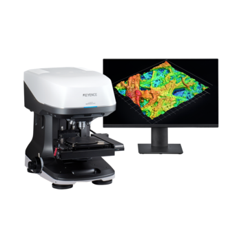
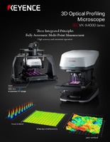
3D Optical Profiling Microscope
White Light Interferometer: A Precision Tool for Engineers in Surface Metrology
Key Takeaways
- Nanometer Precision: Measures step heights and roughness with sub-nanometer vertical resolution.
- Fast 3D Mapping: Captures full 3D surface topography data rapidly—ideal for R&D, and quality inspection workflows.
- Non-Destructive Measurement: Eliminates risk of surface damage making it perfect for polished optics, wafers, and coated parts.
- Versatile Applications: Used in machining, semiconductors, optics, coatings, and additive manufacturing for 3D surface evaluation.
- What to Consider for Adoption: Measurement resolution vs. scanning area, material shape, composition and complexity.
In engineering and precision manufacturing, surface metrology is a cornerstone of quality control and product performance. Among the tools available today, the white light interferometer (WLI) stands out for its ability to deliver non-contact, nanometer-scale surface measurements with exceptional repeatability and speed.
For engineers evaluating advanced metrology instruments, understanding how a white light interferometer works and where it outperforms traditional measurement systems is key to choosing the right solution for R&D or inspection environments.
White Light Interferometer at a Glance
| Category | Details |
|---|---|
|
Category
Technology Type
|
Details
White light interferometry
|
|
Category
Measurement Mode
|
Details
Non-contact, 3D surface topography
|
|
Category
Light Source
|
Details
Broadband (white) low-coherence light
|
|
Category
Vertical Resolution
|
Details
Sub-nanometer (typically < 1 nm)
|
|
Category
Typical Scan Range
|
Details
Up to several millimeters (depending on objective)
|
|
Category
Core Principle
|
Details
Detects interference between reflected light from the sample and a reference mirror
|
|
Category
Key Advantages
|
Details
High precision, non-destructive, fast 3D mapping, ISO-compliant parameters
|
|
Category
Common Applications
|
Details
Semiconductor wafers, machined parts, optical lenses, MEMS, coatings
|
|
Category
Ideal For
|
Details
Engineers and metrologists requiring high-resolution, quantitative data on flat surfaces
|
|
Category
Output Data
|
Details
3D height maps, roughness values (Ra, Sa), step height, and form error
|
Get detailed information on our products by downloading our catalog.
View Catalog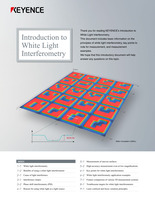

What Is a White Light Interferometer?
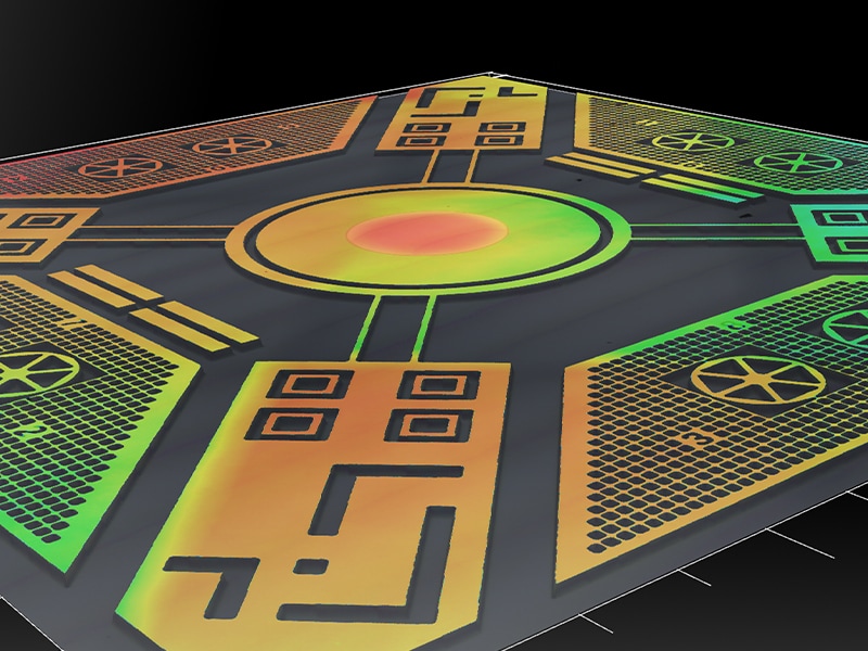
White light interferometry is a non-contact measurement technology that quantifies surface topography with nanometer-level precision by using interference patterns of white light. The technique, also known as vertical scanning interferometry (VSI), produces three-dimensional topographic maps that reveal micro- and nanoscale surface features, making it an indispensable tool for quality control and R&D across diverse applications, from semiconductor wafers to precision-machined components.
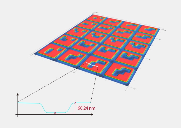
Wafer micropattern (2500×)
Unlike stylus-based profilometers that make physical contact with the surface, WLIs operate entirely optically, eliminating the risk of surface damage while enabling faster, higher-resolution measurements.
For engineers comparing metrology tools, WLI provides an ideal balance between accuracy, non-contact measurement, and automation compatibility.
Technical Background: The Evolution of Interferometric Metrology
Interferometry has its roots in classical physics, with early experiments by Albert Michelson demonstrating how light wave interference could be used to measure distances with extraordinary precision.
Traditional monochromatic interferometers offered sub-nanometer resolution but struggled with real-world engineering surfaces, particularly those that are rough, sloped, or partially reflective.
The introduction of low-coherence, broadband light sources led to white light interferometry, which resolved these challenges. By analyzing interference across multiple wavelengths, WLI systems can now measure a wide range of materials and geometries, from polished optics to machined metals and semiconductor wafers.

How a White Light Interferometer Works
Broadband Light Source
The system emits white light from a low-coherence source (e.g., halogen lamp or LED), containing multiple wavelengths.
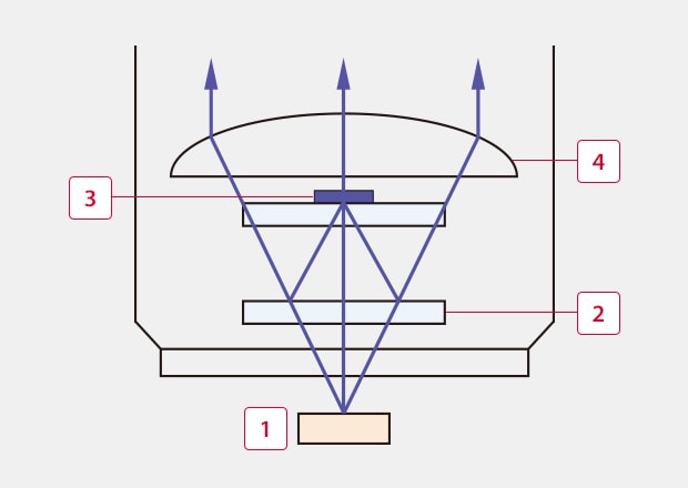
Beam Splitting
Light from the source is divided into two paths by a beam splitter: a reference path and a measurement path. In the VK-X4000 Series, this optical system is optimized to minimize light loss, ensuring a stable interference signal even from samples with low reflectivity.
-
1Target
-
2Beam splitter
-
3Reference mirror
-
4Objective lens
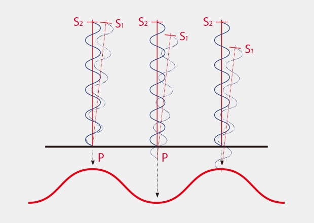
Interference Formation
The two beams reflect and recombine. The resulting interference pattern depends on the optical path difference *1 between the reference and the surface.
*1 Optical path difference = S2P – S1P
Objective lens scanning and interference stripe intensity
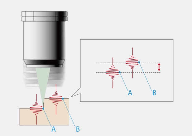
Vertical Scanning
The interferometer’s objective or stage moves vertically, scanning through focus. The point of maximum fringe contrast identifies the exact height of each pixel on the surface. The difference between the interference intensity peaks at points A and B indicates the height difference.
Surface Reconstruction
The instrument’s software compiles this data into a 3D surface map, providing quantitative information about roughness, step height, and form.
For engineers, this principle means traceable, repeatable data without mechanical contact—ideal for validating precision components and ensuring process stability.

Why Engineers Choose White Light Interferometry
White light interferometers are valued by engineering teams because they combine microscopic visualization with metrological accuracy.
Key Advantages
- Non-contact operation — Eliminates stylus wear and surface damage.
- Nanometer-level vertical resolution — Detects subtle surface variations critical for performance parts.
- Fast acquisition speed — Supports batch inspection and process feedback.
- Versatility — Suitable for smooth, rough, or patterned surfaces across metals, polymers, and ceramics.
- Quantitative output — Generates ISO-compliant surface parameters (Ra, Rz, Sa, Sq).
Engineering Applications
In metrology labs, WLI systems provide the data traceability and measurement certainty engineers rely on for process validation and certification.
- Process development — Validate machining, polishing, or coating processes.
- Failure analysis — Detect wear, corrosion, or fatigue-related surface changes.
- Optical component testing — Measure lens curvature, coating thickness, and form error.
- Microelectronics — Analyze wafer flatness, MEMS structures, and thin film layers.
- Additive manufacturing — Assess surface integrity and build consistency layer by layer.
Application Examples
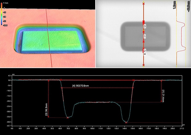
Plastic micro-shape measurement
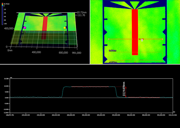
Film thickness measurement

Comparing WLI to Other Metrology Tools
For engineers, white light interferometry often represents a good compromise between resolution, speed, and usability, particularly when both fast acquisition and high-resolution are required.
| Technique | Type | Measurement Speed | Material and Slope Compatibility | Key Strength | Limitations |
|---|---|---|---|---|---|
|
Stylus Profilometer
|
Type
Contact
|
Measurement Speed
Line speed fast. Area speed slow.
|
Material and Slope Compatibility
Good for hard, semi-flat surfaces. Struggles with very rough, porous, or fragile/soft materials and slopes > 70°.
|
Key Strength
Simple, accurate, established.
|
Limitations
Can damage surface; limited to 2D profiles (unless integrated with motorized stage); material limitations. Unable to provide true-color data of surface.
|
|
Confocal Microscope
|
Type
Optical
|
Measurement Speed
Moderate.
|
Material and Slope Compatibility
Works on any material and any shape/slope approaching 90°.
|
Key Strength
Good for high-resolution imaging + material/shape independent.
|
Limitations
Limited to area viewed by objective lens (unless stitching); slower acquisition.
|
|
White Light Interferometer
|
Type
Optical
|
Measurement Speed
Very fast area scanning.
|
Material and Slope Compatibility
Good for flat surfaces with high reflectivity. Struggles with slopes >= 25° depending on objective used.
|
Key Strength
Achieves both nanometer-order vertical resolution and rapid 3D mapping, often in seconds.
|
Limitations
Cannot measure features that are optically inaccessible, such as undercuts or internal structures. Specialized techniques may be required for materials that have extremely low-reflectivity.
|
|
AFM (Atomic Force Microscope)
|
Type
Contact
|
Measurement Speed
Very slow.
|
Material and Slope Compatibility
Most materials, including biological but must be incredibly flat. Struggles with soft or sticky materials.
|
Key Strength
Atomic-scale resolution.
|
Limitations
Small scan area; very slow scanning; very flat surfaces. Typically requires a lot of work for preparing samples to be scanned. Unable to provide true-color data of surface.
|
Engineer’s Buyer’s Guide: How to Choose the Right White Light Interferometer
When selecting a white light interferometer, engineers should evaluate both technical performance and integration fit. The right instrument depends on the intended application, measurement scale, and workflow requirements.
- Vertical Resolution and Measurement Range
- Check the system’s z-resolution (typically sub-nanometer) and its vertical scanning range. A higher range is ideal for parts with curved surfaces or significant height variation.
- Objective Lenses and Field of View
- Choose magnification levels that balance resolution and coverage area. Some systems allow rapid objective switching for multi-scale measurements.
- Surface Type Compatibility
- Consider surface reflectivity, roughness, and transparency. Systems with adaptive light intensity or specialized objectives handle a broader range of materials.
- Stage and Automation Options
- Motorized XYZ stages and stitching capabilities allow engineers to measure larger samples automatically or combine multiple scans into one dataset.
- Software and Data Analysis
- Evaluate the software’s ability to calculate surface parameters (Ra, Rq, Sa, etc.), generate ISO-compliant reports, and export data to CAD, SPC, or simulation tools.
- Application Versatility
- Engineers rarely measure just one type of sample, so it’s essential to choose equipment that can handle the full range of materials and geometries you encounter. Consider whether the system can reliably measure diverse surfaces—different material types, curved or cylindrical parts, steep slopes, coatings, and thin films. Can it also provide high-resolution imaging alongside measurement? And if you routinely analyze similar sample types, could automation streamline your process?
A clear understanding of your requirements helps reduce long-term costs by limiting the number of systems you need and simplifying your overall workflow.
By aligning these specifications with measurement objectives, engineers can ensure that their investment in WLI technology delivers accurate, repeatable, and actionable data for their processes.

Conclusion
For engineers evaluating metrology solutions, the white light interferometer represents a proven and precise technology. Its combination of optical interferometry, non-contact operation, and fast acquisition makes it indispensable for industries that demand both accuracy and efficiency.
Whether you’re optimizing a precision manufacturing process, validating microfabricated components, or conducting advanced surface research, white light interferometry delivers the quantitative confidence and measurement traceability that engineering workflows depend on.
For more information on interferometers, including technical details, please visit our White Light Interferometers page.
You can also download our Introduction to White Light Interferometry guide below.