3D Optical Profiling Microscope
Easy and Accurate Measurement of Chip Components
-
Tags:
- Electronic Devices , PCBs
Recent PCB mounting technologies are becoming denser and more complex in response to the need for smaller, lighter, and thinner information terminals, such as smartphones and home electronics, and also smaller electronic components, such as chip resistors and ceramic capacitors. This section introduces problems that can occur with mounted components, as well as how 3D measurement systems can be used to evaluate, analyze, and prevent these problems.

Chip Component Mounting Method
Along with the miniaturization of electronic components and higher density of PCB mounting, reflow soldering has become mainstream.
| Soldering method | Characteristics | |
|---|---|---|
| Advantages | Disadvantages | |
|
Soldering iron
|
Advantages
Low thermal stress
|
Disadvantages
Large temperature fluctuation
|
|
Hot air
|
Advantages
Low thermal stress
|
Disadvantages
Large temperature fluctuation
|
|
Laser
|
Advantages
|
Disadvantages
Not suited for mass production (long processing time)
|
|
Pulse heat
|
Advantages
|
Disadvantages
Not suited for mass production (long processing time)
|
|
Reflow (infrared type)
|
Advantages
|
Disadvantages
|
|
Reflow (hot air type)
|
Advantages
|
Disadvantages
|
|
Flow soldering
|
Advantages
|
Disadvantages
|
What is Reflow Soldering?
Solder paste, which is a uniform mixture of powdered solder and flux, is applied onto a metal plate with holes punched in it, and spread into a thin layer with a spatula to make a print. Components are then mounted on the circuit board, heated, and soldered.
1. Solder Printing

To print pad shapes, solder paste is applied onto a metal plate and spread into a thin layer.
2. Component Mounting

Components are mounted on the circuit board with a device known as a chip mounter.
If the number of components is small, it is also possible to perform component mounting by hand.
3. Heating and Cooling

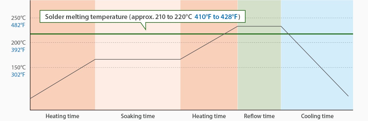
A reflow oven is used to apply heat at or above the melting point of the solder. After soldering is complete, the targets are cooled.
The temperature is controlled in five steps (see the section below).
Reflow Furnace Temperature Control
Normally, heat is applied in two steps. In the first heating step, the circuit board is brought to and maintained at a uniform temperature. In the second heating step, the solder paste melts. The heating temperature and time vary depending on the type of reflow oven and on the components being used.
Problems in Surface Mounting
Misalignment
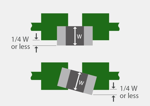
The component is misaligned and protrudes by 1/4 of its width W or 1.5 mm 0.06″ or more from the side.
Looseness
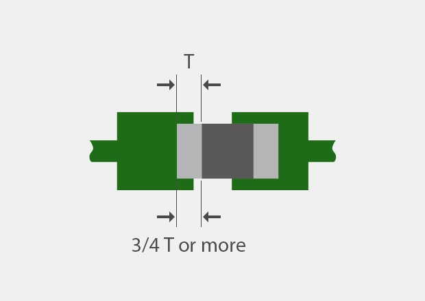
The contact of the electrode of the component is less than 3/4 of its width T.
Tilt
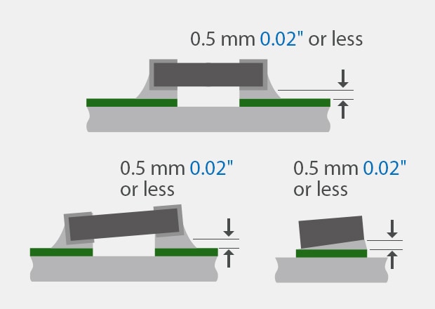
The component body is tilted or higher than the specified dimension (0.5 mm 0.02″) from the PCB.
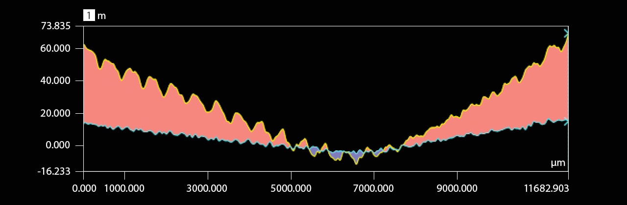
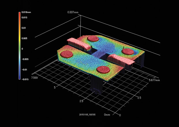
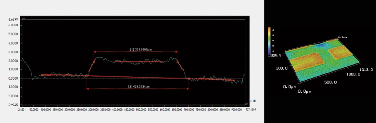
Example of Circuit Board Warpage Measurement
PCB warpage is caused by temperature changes that occur when power is supplied, or by environmental changes. Analysis is performed to determine whether defects have occurred due to these temperature changes. Warpage caused by temperature fluctuations can be measured from room temperature to 260°C 500°F.
Reference image
Comparison image
One profile from two specified points
Get detailed information on our products by downloading our catalog.
View Catalog

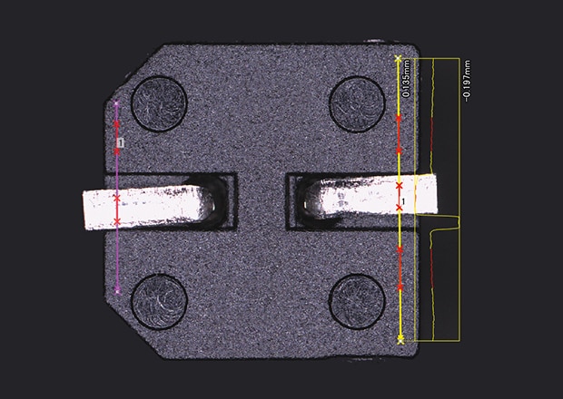
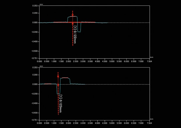
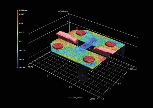
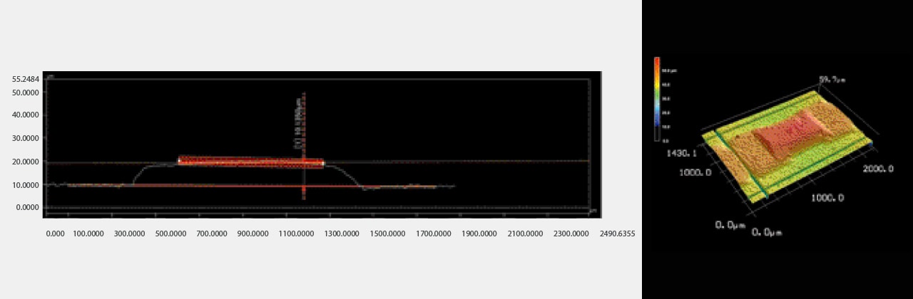
Coplanarity Measurement Example of the Terminals of an Aluminum Electrolytic Capacitor
The flatness of capacitor terminals, which can lead to PCB mounting defects and can influence the mounting strength of the PCB, can be measured.
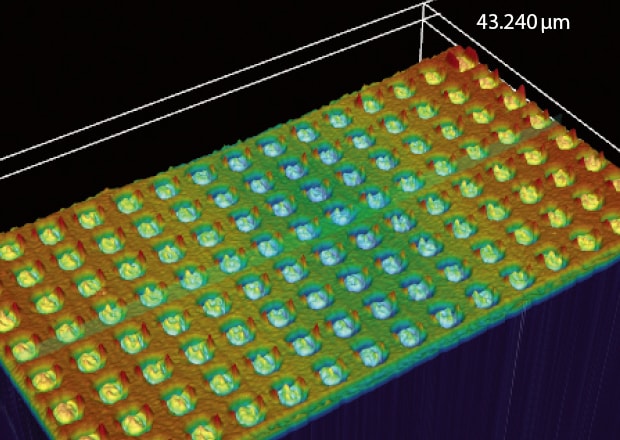
Example of Solder Paste Thickness Measurement
The thickness of the solder layer applied on a PCB can be measured.
Get detailed information on our products by downloading our catalog.
View Catalog
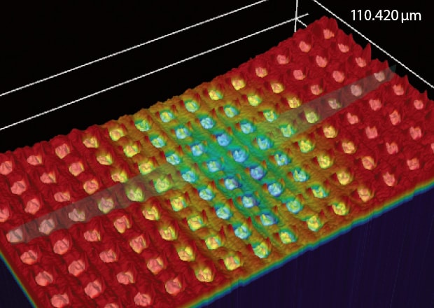
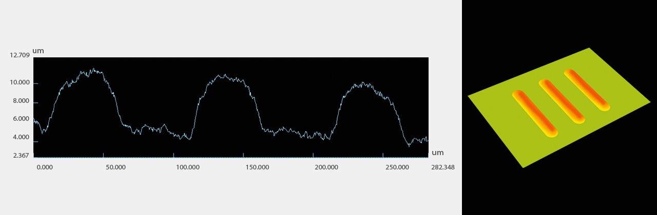
Examples of Resistive Film Thickness Measurement
The thickness and volume of a resistive film in a wet state can be measured prior to sintering after the film has been printed. The film thickness can be measured while it is wet, so the conditions for the sintering process can be set efficiently.
Chip Resistor Structure
Chip resistors are small, square fixed resistors consisting of a resistive element formed on the surface of an insulating base, such as ceramic, with electrodes on both ends. They are mainly suited for surface mounting.
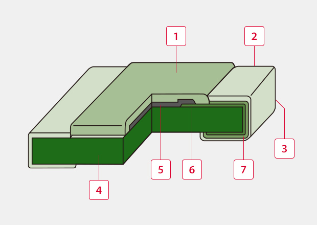
Typical Structure of a Square Chip Resistor
The square chip resistor has no lead wires on the terminal electrodes and can be soldered or bonded.
MELF-type resistors with cylindrical shapes are also available, but they are not commonly used.
-
1Protective film
-
2Exterior plating
-
3Terminal electrode
-
4Ceramic
-
5Resistive film
-
6Internal electrode
-
7Nickel plating
Ceramic (base)
The base is made of a ceramic plate to endure sintering or trimming of the resistive element.
Resistive element
There are thick- and thin-film types.
Electrode
The resistive element is connected to the terminal electrodes via internal electrodes. It has a structure of at least three layers.
Protective film
The surface of the resistive element is coated with resin or glass to prevent direct adhesion of moisture or dust.

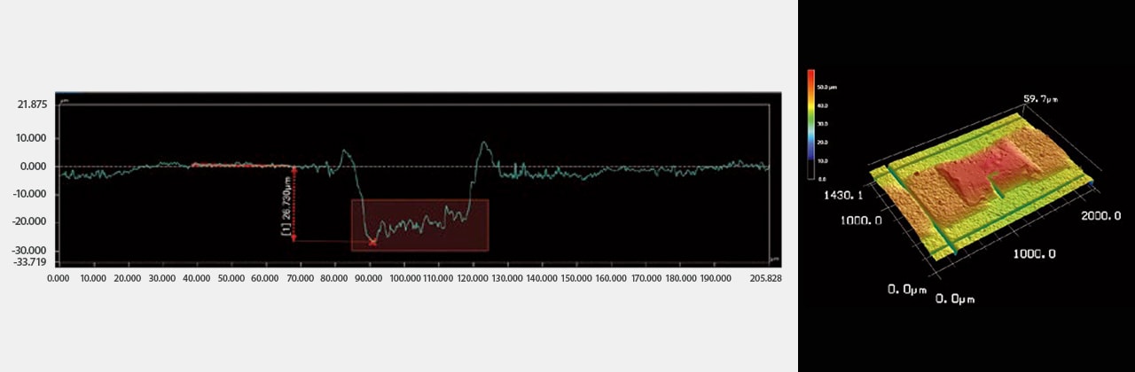
Depth Measurement Example of Cracks in Films
The length and depth of films can be measured to ensure that chip resistors remain within specification.
The width and depth of cracks that occur in trimmed areas can also be measured.
Laser Trimming
The layers of a chip resistor are formed by screen printing. Since several hundreds of resistive elements are formed on a ceramic base, even minute variations in the printing conditions directly cause variations in the resistance.
If the resistance varies among chip resistors, their electrical characteristics will not satisfy their rating. This leads to the need to perform laser trimming to adjust the resistance. Laser trimming involves measuring resistive elements one by one, and cutting them to ensure the specified resistance and to minimize variations.
- Resistive elements are printed by aiming for a slightly lower resistance than the target resistance.
- Trimming a resistive element makes its current path narrower, which increases resistance.
- Trimming stops when the target resistance is achieved to minimize fluctuation among chips.
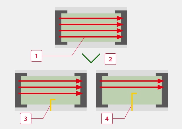
Illustration of increasing resistance
* As the element is trimmed further, the current path in the resistive element becomes narrower which increases the resistance.
-
1Flow of electric current
-
2Laser trimming
-
3A short trimming length causes a small change in the resistance
-
4A long trimming length causes a large change in the resistance
The final trimming length and shape are determined based on the change in the resistance during trimming.
When the changes in the resistance based on the cut length are compared between straight cutting and L-shape cutting, L-shape cutting can provide higher accuracy at the final cut and reduce the influence of micro cracks at the end.
Straight cutting
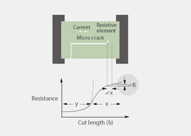
L-shape cutting
Dielectric Width Measurement
The pattern width and thickness of a dielectric in a wet state can be measured.
Structure of a Multilayer Ceramic Chip Capacitor
The basic structure of a capacitor consists of a dielectric between two electrode plates.
- Dielectric material such as barium titanate (BaTiO3), a ceramic dielectric, is applied to a carrier film.
- The material is dried to create a thin sheet.
- Paste of electrode material containing metals such as palladium, silver, or nickel, is printed on the sheet.
- The sheets are stacked in 10 to 1000 layers, pressed and cut into chips.
- The final steps in creating multilayer ceramic chip capacitors are sintering and plating external terminals with silver. The chips shrink by around 10% during the sintering of the ceramic, which is important to take into account when determining their dimensions.
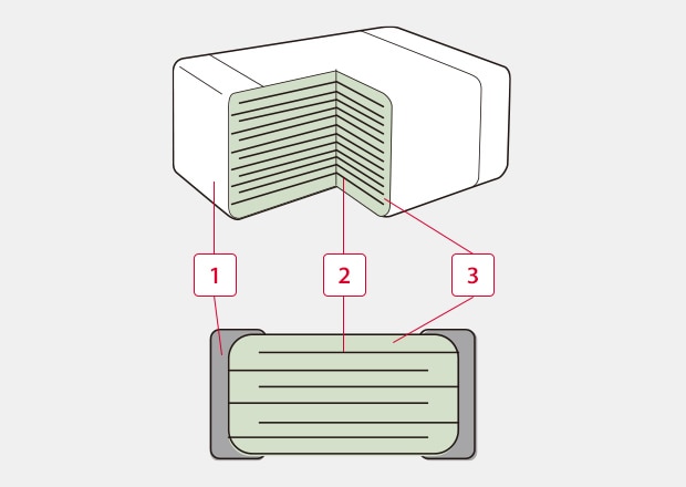
-
1External electrode
-
2Internal electrode
-
3Ceramic dielectric
Proportional Relationship Between Electrostatic Capacitance and Electrode Plate Area
Connecting multiple capacitors in parallel is equivalent to increasing the area of the electrode, so you can increase the electrostatic capacitance by increasing the number of capacitors.
Using multiple capacitors will take up a large volume on the circuit board, so this method is not appropriate when there is a need to save space.
To avoid this, multilayer ceramic chip capacitors achieve both miniaturization and large capacity by having multi-layered structures of ceramic dielectrics and internal electrodes stacked alternately.