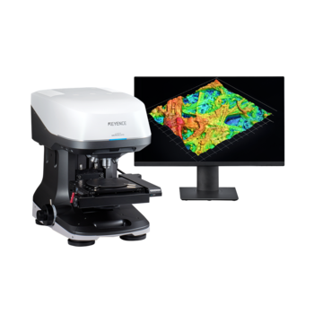
3D Optical Profiling Microscope
3D Measurement Applications of Integrated Circuits (ICs)
-
Tags:
- Electronic Devices , PCBs
The popularity of 5G as a standard for cellular networks has lead to the miniaturization of semiconductor devices, which in turn has increased the need for precise inspection and analysis. The latest features of KEYENCE's VK-X4000 Series allow it to perform repeated measurements, location-based programs, and pass/fail inspection through templating. This section introduces technical information and inspection application examples for BGA, wire bonding, contact probes, and similar cases where many inspections are carried out with laser microscopes.

Typical IC Packages
As the integration of ICs has increased, Surface Mount Technology (SMT) has become mainstream. Matrix type (BGA type) packages are also used for highly integrated ICs. LSI is an acronym for Large Scale Integration but is often used as a synonym for Integrated Circuits (IC).
Insertion Type Package
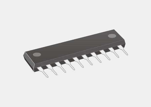
SIP (Single Inline Package)
These packages are inserted into PCBs. Leads are extended from the long side of the package in a line.
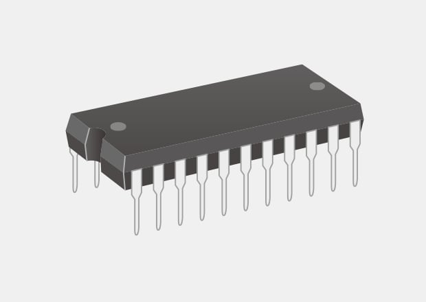
DIP (Dual Inline Package)
These packages are inserted into PCBs. Leads extend downward from both sides of the package.
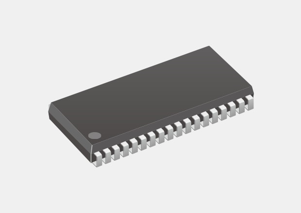
Surface Mount Technology (SMT) Lead Type Package
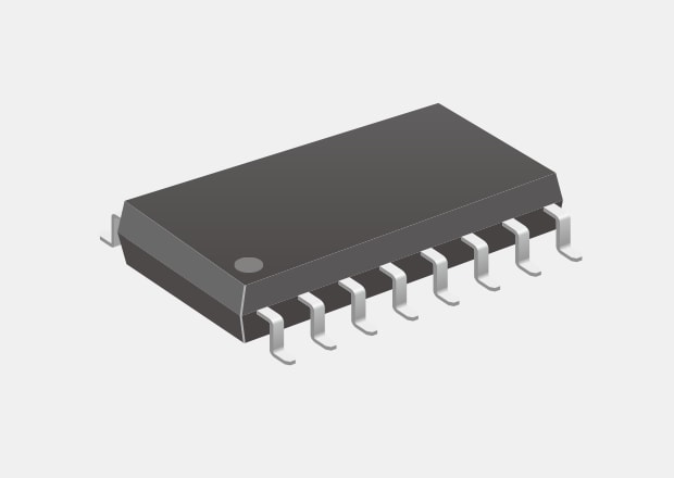
SOP (Small Outline Package)
In these SMT packages, leads extend from both sides of the package and the tips of the leads spread out like wings.
SOJ (Small Outline J-Leaded Package)
In these SMT packages, leads extend from both sides of the package and tips of the leads are bent inward, as if they cover the package. When viewed from the side, each lead looks like the letter J.
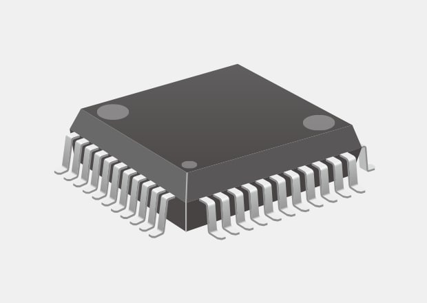
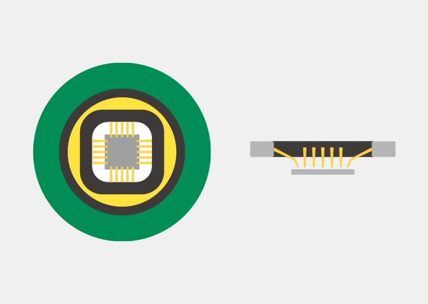
QFP (Quad Flat Package)
In these SMT packages, leads extend from all 4 sides of the package and tips of the leads are spread like wings.
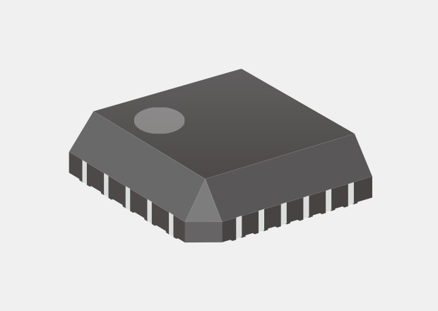
QFJ (Quad Flat J-Leaded Package)
In these SMT packages, leads extend from all 4 sides of the package and the tips of the leads are bent inward, as if they cover the package.
When viewed from the side, each lead looks like the letter J.
Surface Mount Technology (SMT) Non-Lead Type Package
SON (Small Outline Non-Leaded Package)
These SMT packages have no leads. Electrode pads are used as connection terminals. SON are used for two-way types and for small numbers of pins.
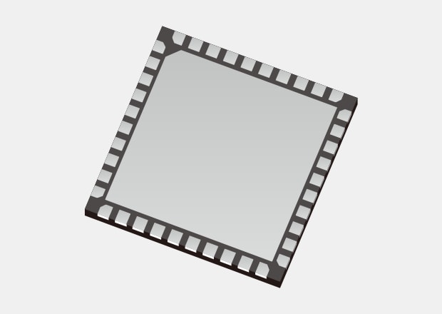
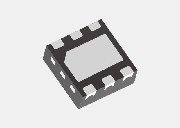
QFN (Quad Flat Non-Leaded Package)
These SMT packages have no leads. Electrode pads are used as connection terminals. QFN are a four-way type package.
Surface Mount Technology (SMT) Matrix Type Package
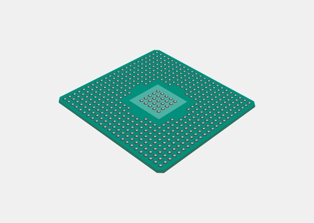
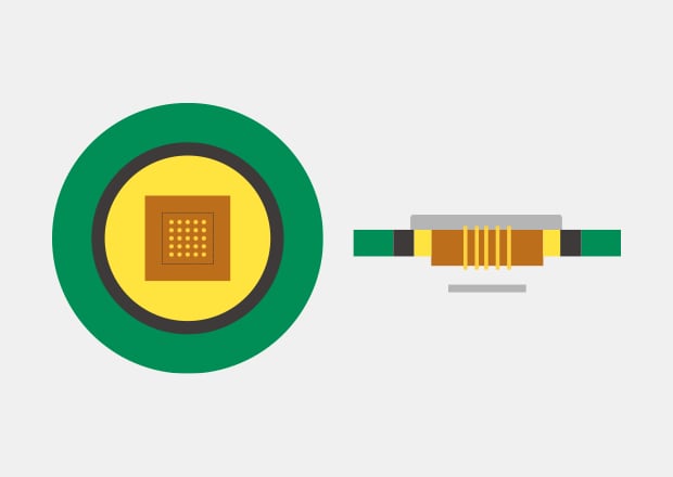
BGA (Ball Grid Array)
Solder balls (sphere shaped) are arrayed on the bottom of the package to use as terminals.
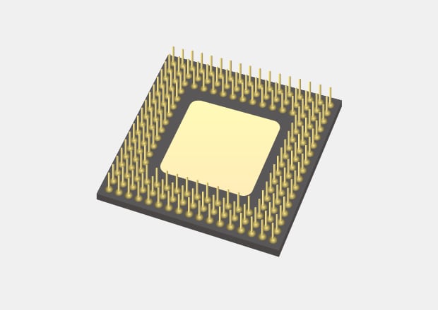
PGA (Pin Grid Array)
Pins are arrayed on the bottom of the package to use as terminals.
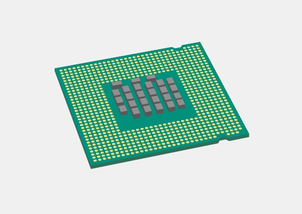
LGA (Land Grid Array)
Electrode pads (including copper pads) are arrayed on the bottom of the package to use as terminals.

Typical Bonding for IC Chip Mounting
Wire Bonding
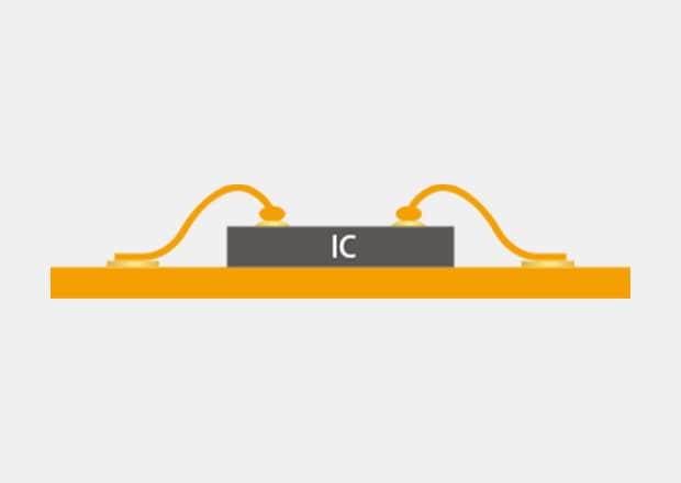
Wire bonding connects electrodes of semiconductor chips and electric conductors of lead frames or boards with thin wires of gold, aluminum, or copper.
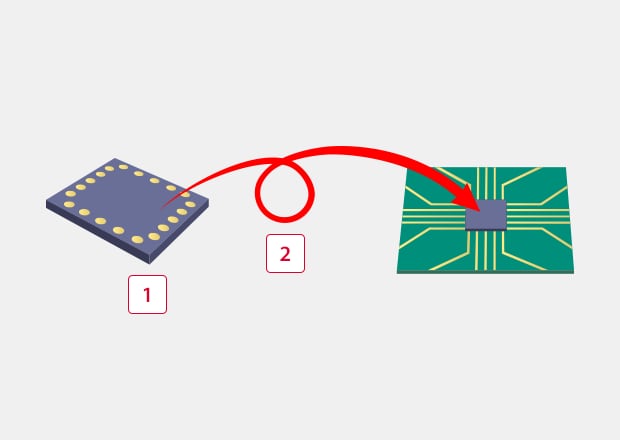
Flip-Chip Bonding
IC chips are attached directly to PCBs. This method is called FC-BGA (Flip Chip-BGA). Bumps are made at the electrodes of an IC chip and connected to the electrodes of a PCB. Using this method can save space compared to wire bonding.
-
1Semiconductor chip
-
2Flip (Face down)
Bump Making Methods for Flip-Chip Bonding
Solder Ball Mounting
Solder balls (made in advance) are placed on electrodes and reflowed to make bumps. Higher bumps can be made possible paste printing. Also, standardizing the solder ball size prevents final bump height differences.
Paste Printing
Solder paste is printed on electrodes and reflowed to make bumps. Throughput is high, but it is difficult to unify the bump height.
Plating
Solder bumps are formed with electroplating. Fine bumps can be made, but throughput is low.
Wire Bonding Flow
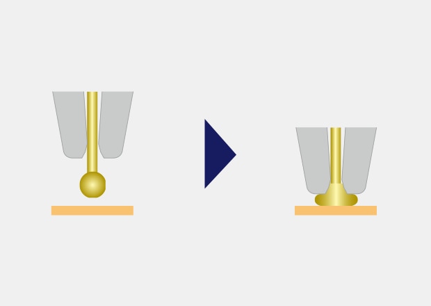
Tube shaped capillaries (like an injection needle) with metal wires running through them are used. The wire tip is sparked by high voltage to make it round. The round part is then bonded to the electrode to attach it. This is called Ball Bonding or 1st Bonding. A load from the capillary, ultrasonic waves, and heat from the bonding stage allow the bonding to take place.
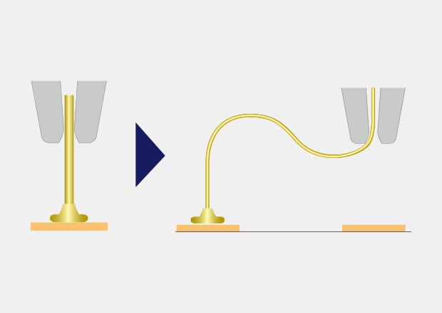
The capillary is moved to the 2nd bonding point by pulling the bonding wire in a continuous loop.
When connecting to a lead electrode, no ball is made and the wire is mashed by the capillary. This is called "Stitch Bonding" or "2nd Bonding."
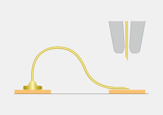
The wire clamper is closed to clip the metal wire, then the capillary is lifted and the wire is cut.
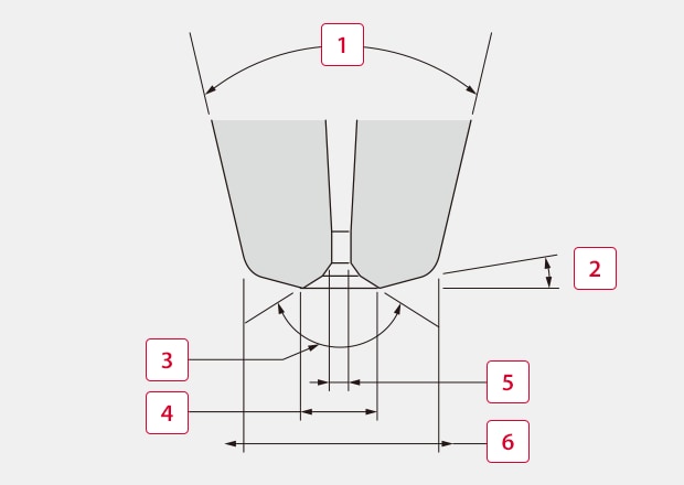
Capillary Tip Components
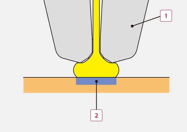
1st Bonding
-
1Capillary
-
2Bonding part
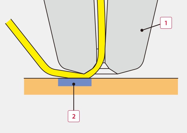
2nd Bonding
-
1Capillary
-
2Bonding part
-
1Cone angle
-
2Face angle
-
3Chamfer angle
-
4Chamfer diameter
-
5Hole diameter
-
6Tip diameter
Wire Bonding Inspection Examples
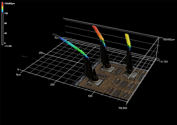
Wire bonding 3D image
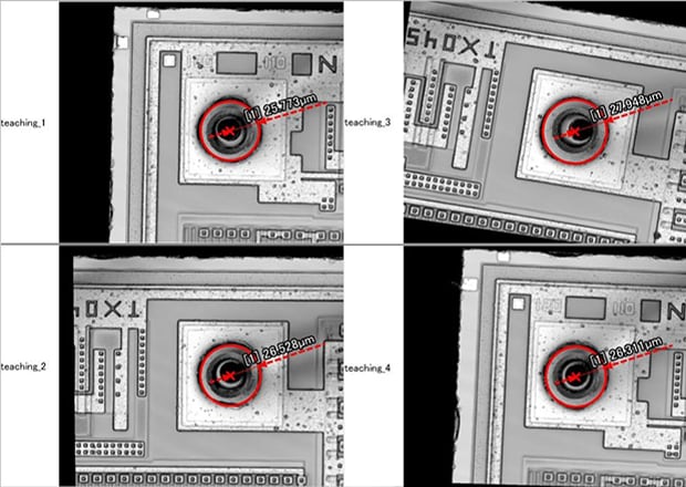
Wire bonding teaching for automatic measurement
Even if the target shifts out of position, the position is corrected automatically, allowing for automatic measurement.
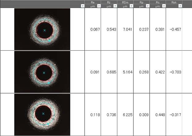
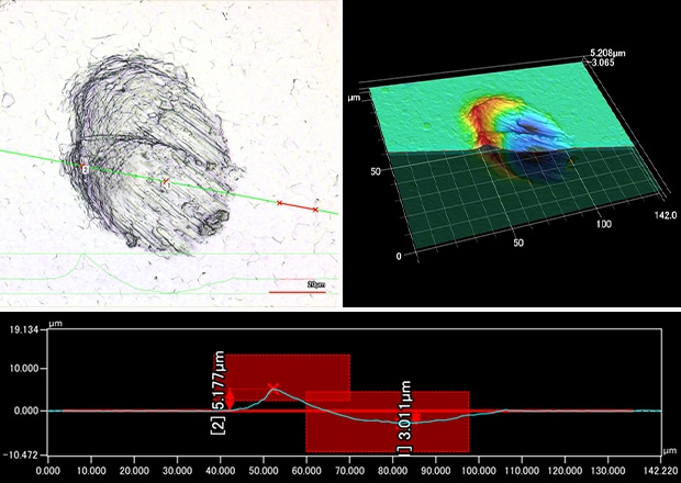
Capillary tip roughness measurement (Multiple measurements)
The batch analysis function can be used to optimize inspections.
Get detailed information on our products by downloading our catalog.
View Catalog
IC Inspection Examples
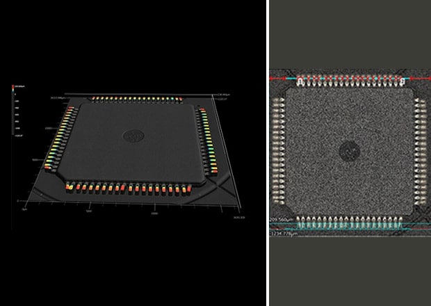
Terminal coplanarity measurement
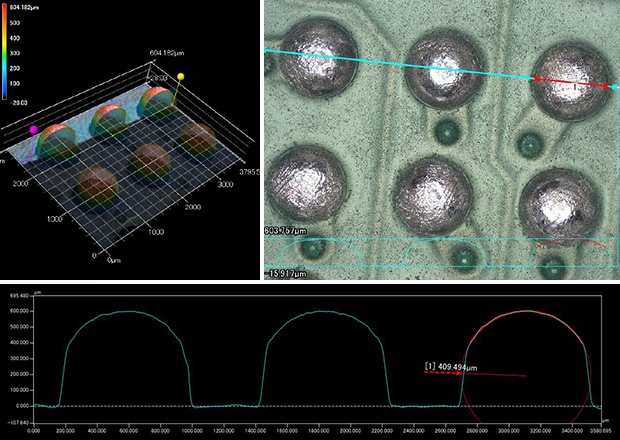
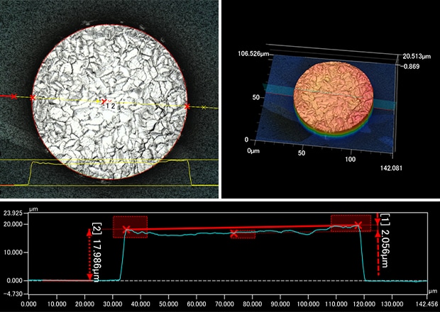
BGA shape measurement
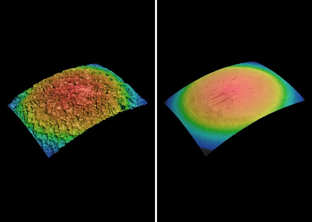
BGA surface roughness comparison
Bump outer diameter and height measurement
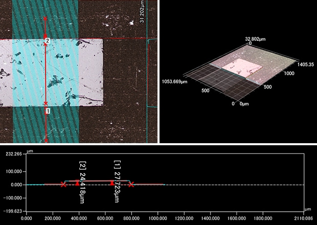
Resist film thickness measurement
Electrode height measurement
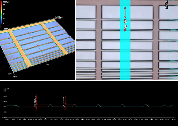
Smartphone PCB pattern measurement
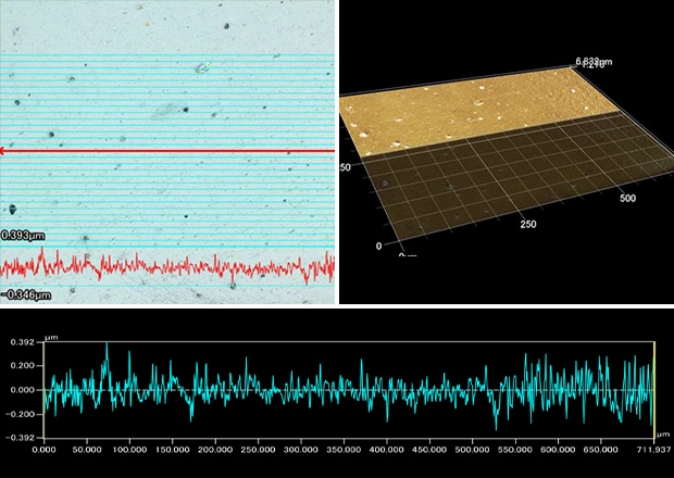
Roughness measurement for multiple lines of an IC package
The recommendation function clarifies the roughness parameter that should be used during incoming inspections.
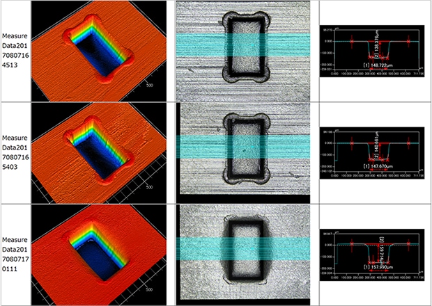
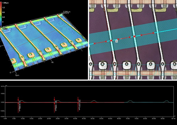
Carrier tape shape measurement
Batch analysis enables automatic measurement.
Get detailed information on our products by downloading our catalog.
View Catalog
Electrical Inspection Methods
This section introduces typical electrical inspection methods for electronic components. In addition to simply opening or shortcircuiting a component, it is also possible to make current flow through a component.
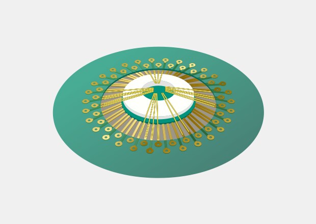
Probe Card
This is a jig used during electric inspection of LSI (large scale integration) chips formed on top of silicon wafers in the wafer inspection process (pre-processing) as part of manufacturing LSI circuits.
Contact Probe
This is a jig used during inspection of various electronic components. This inspection targets a wide variety of components including semiconductors, LCD panels, raw PCBs, mounted PCBs, connectors, capacitors, and sensors.
Probe Card Types
Vertical Probe Card
With this probe card, a block with a probe affixed vertically is attached to the PCB.
[Advantages]
- User-defined probe arrangement (square-block type, suitable for measurement of multiple components)
- Easy maintenance (Replacement of a single probe is possible.)
- Small scratches
- No damage to solder
[Disadvantages]
- High price
- Difficult to use with aluminum pads
Cantilever Probe Card
With this probe card, needles made of tungsten or a similar material are fixed in place directly on the PCB.
[Advantages]
- Low price
- Allows for narrower pitches than vertical probe cards
- Easy to use with aluminum pads
[Disadvantages]
- Limited pin layout
- Maintenance is difficult (Height adjustment and other repairs are required.)
- Large scratches
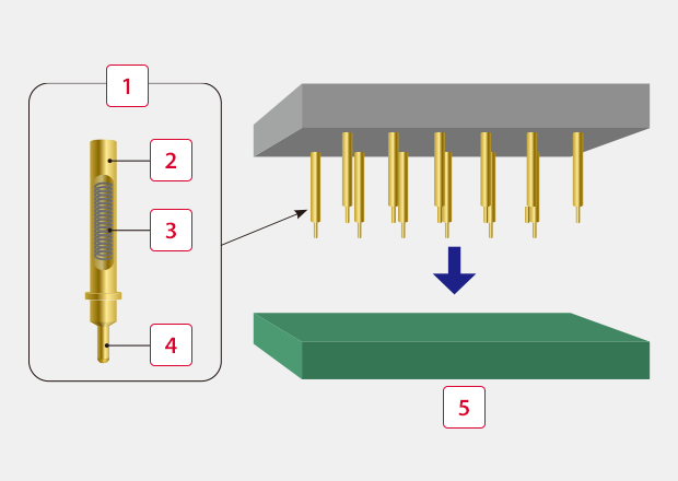
Contact Probe Structure and Tip Shapes
A contact probe is constructed from a plunger, barrel, and spring, and is used while embedded in a jig made of resin.
-
1Contact probe
-
2Barrel
-
3Spring
-
4Plunger
-
5Inspection target
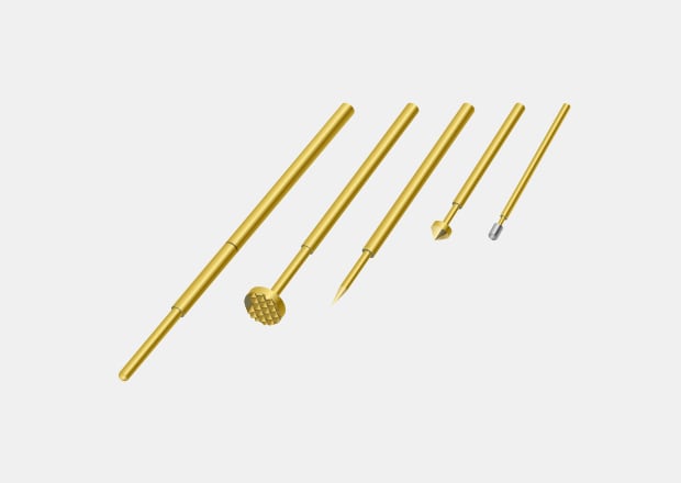
Curve
Used with flexible PCBs and in other situations where damage to electrodes must be avoided.
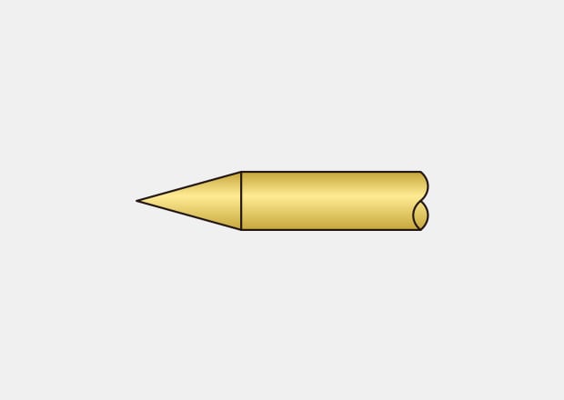
Needle
Used mainly with PCB pads and similar targets.
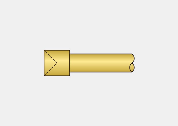
Flat and Inverted Cone
Flat tips are used to contact the surface without damaging the electrodes. Inverted cone tips are used to receive terminals and similar targets.
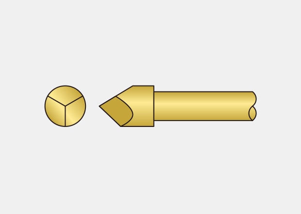
Triangular Pyramid
Used with PCB through-holes and similar targets.
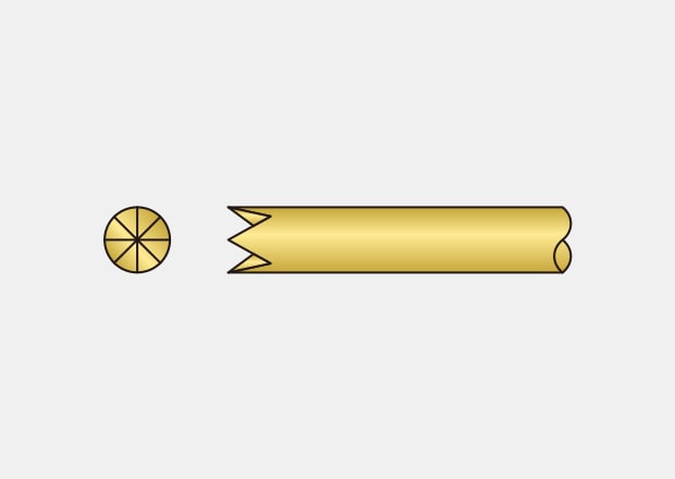
Crown
Used in situations such as contacting multiple points or receiving the leads of mounted components.
Contact Probe Inspection Examples
Probe mark depth measurement
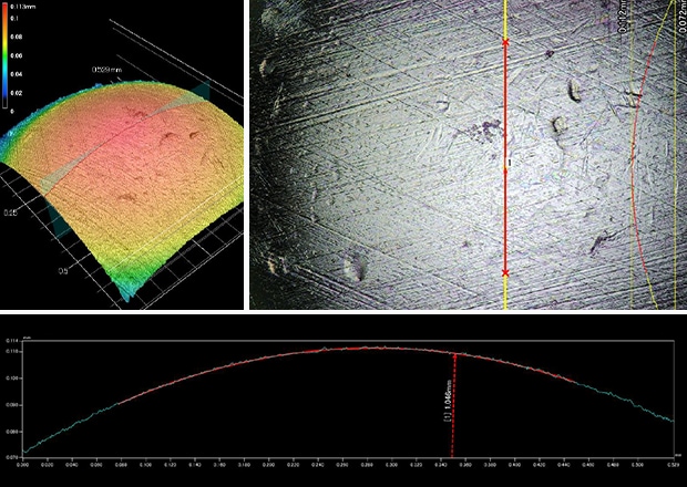
Probe tip wear measurement