3D Optical Profiling Microscope
Instantaneous Measurement of Printed Circuit Boards (PCBs)
-
Tags:
- Electronic Devices , PCBs
In recent years, devices such as smartphones, tablets, and wearables have become smaller, with lower profiles and higher functionality. The PCBs and other components used in these devices have also become smaller, denser, and more multilayered. This has resulted in an increased demand for more detailed product inspection and analysis. KEYENCE’s latest model of the VK-X4000 Series is capable of repeat measurements, automatic measurement of multiple locations of the same target, and creation of OK/NG analysis templates. This section introduces technical information related to PCBs and PCB-mounted components along with example inspections using 3D Optical Profiling Microscopes.

Printed Circuit Board
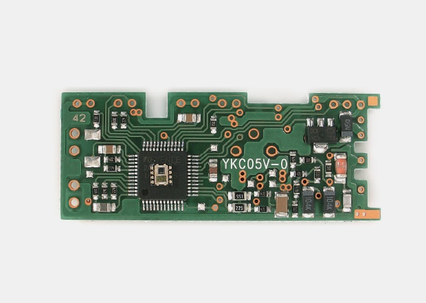
The term PCB is used to refer to printed circuit boards that have components mounted. Boards without mounted components are called PWBs (Printed Wiring Boards).
Types of Printed Boards
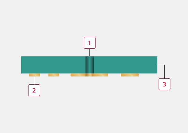
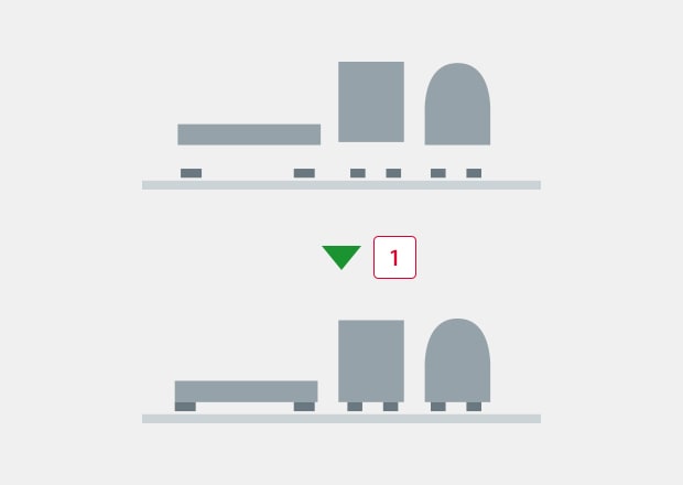
Single-Sided Board (One-Layer Board)
A layer of copper foil is attached on one side of the board.
This type has non-through holes that are made by drilling or punching and aren’t plated. They are mainly used for mass produced electronic appliances for consumer use to reduce production costs.
-
1Non-through hole
-
2Copper foil
-
3Base
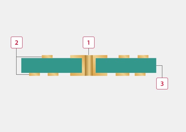
Double-Sided Board (Two-Layer Board)
Copper foils are attached on both sides of the board.
The cost is slightly higher than a single-sided board, but the space for wiring and mounting is doubled, so the size of the board can be smaller. This benefit is why they are widely used for electronic devices.
-
1Through hole
-
2Copper foil
-
3Base
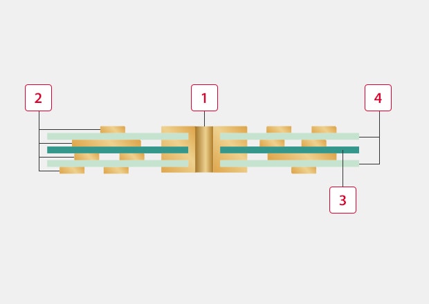
Multi-Layer Board
Multi-layered PCBs include copper foils and insulating layers called prepreg. There are 4-layer, 6-layer, and 8-layer boards. The more layers a board has, the more complicated the structure and the higher the manufacturing cost. Power supply and typical signal lines can be placed inside of the board, which increases the space on the surface and mounting density.
-
1Through hole
-
2Copper foil
-
3Base
-
4Prepreg
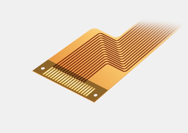
Flexible Board
Flexible boards are commonly used to fit inside moving parts or cases that fold. Film materials, including polyimide, are used for these boards. The boards are thin and have a flexible structure.
PCB and PCB-Mounted Component Inspection Examples
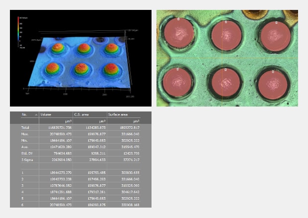
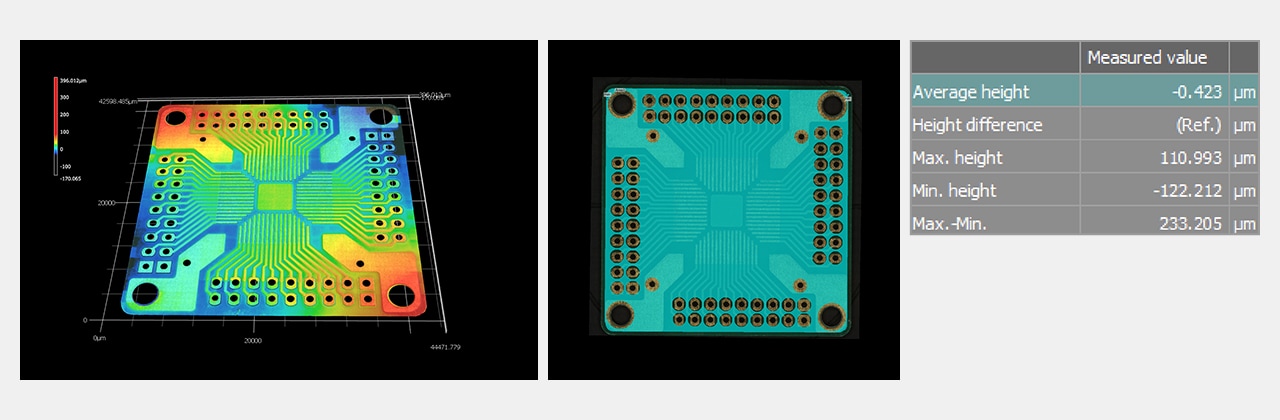
Warpage Inspection
The height color display makes it possible to visualize warpage.
The surface measurement function can also automatically measure the maximum and minimum surface points.
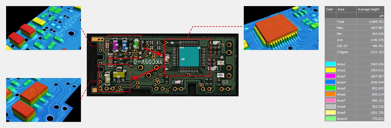
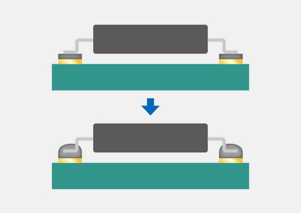
Automatic Inspection of Mounted Component Heights
Focus variation mode allows for automatic inspection of various targets over a measurement area 16 times larger than that of conventional products.

How to Mount PCBs
PCB mounting is the process of bonding electronic parts on a PCB to make electronic circuits.
Soldering is used to bond the parts. There are two methods of bonding: IMT (Insertion Mount Technology) and SMT (Surface Mount Technology).
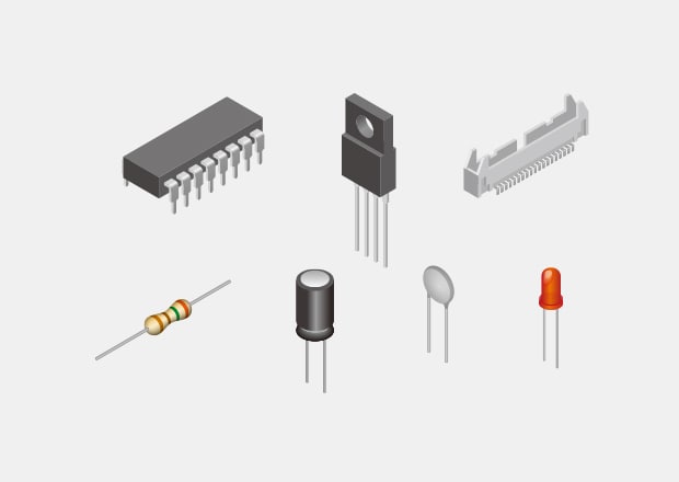
IMT: Insertion Mount Technology
Leads are inserted into through holes on the PCB and soldered. As more components are placed on the board, the board size must be increased. Electronic parts that have leads wired downward from the packages for IMT are called DIP (Dual In-line Package) components.
SMT: Surface Mount Technology
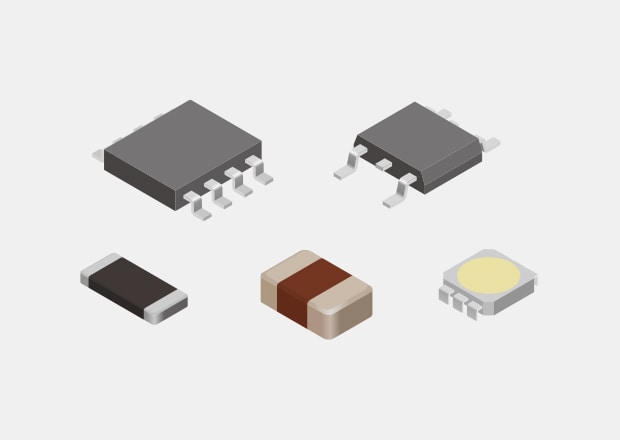
The current mainstream PCB mounting method is Surface Mount Technology (SMT). Electrodes are soldered to pads on PCB surfaces without using through holes. Unlike IMT, the electrodes don’t penetrate, so many components can be mounted on both sides of the PCB, allowing for smaller PCBs. Components mounted without lead are referred to as SMDs (Surface Mount Devices).
Parts of PCBs
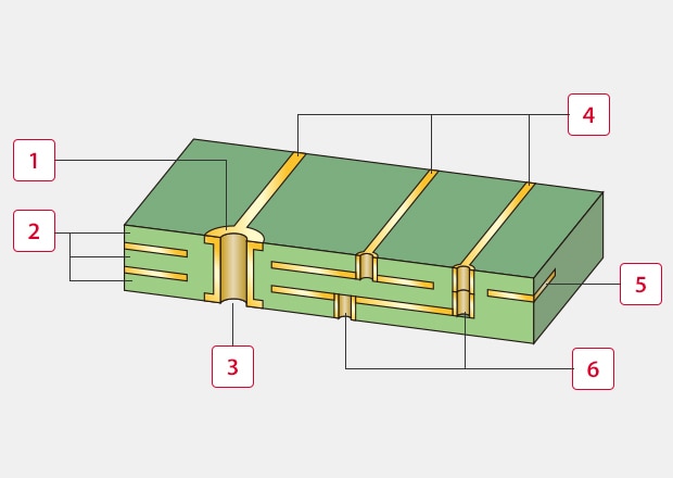
The holes that connect different circuitry layers are called vias. Lands are the surrounding areas of through holes to solder the leads of electronic components.
-
1Land (Pad)
-
2Insulator layer (Prepreg)
-
3Through hole
-
4Track (Pattern)
-
5Plane layer or Wire layer
-
6Via
PCB-Related Inspection Examples
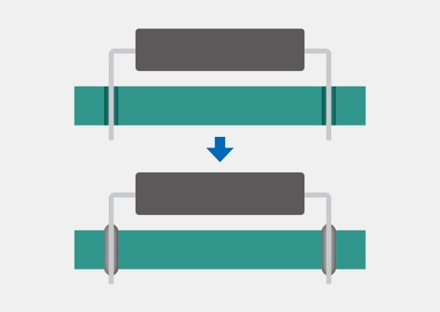
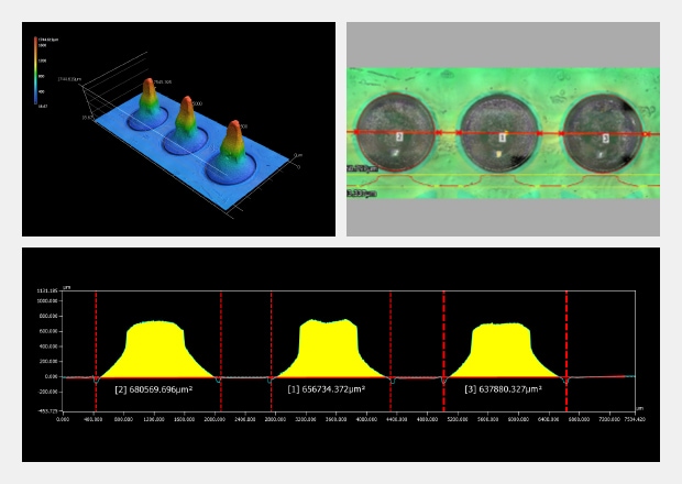
Pattern Height and Cross-Sectional Area Inspection
Measuring the average of multiple lines helps reduce the effects of roughness and scratches.
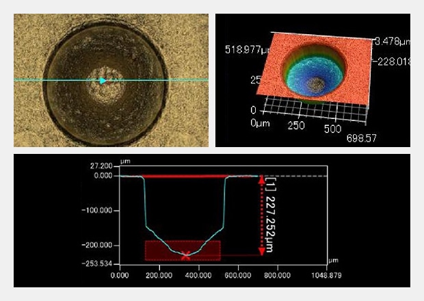
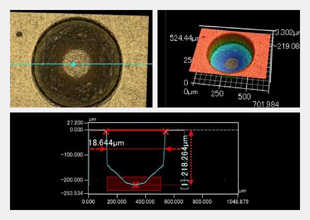
Via Depth Inspection
The automatic measurement function makes it possible to reduce inspection times.
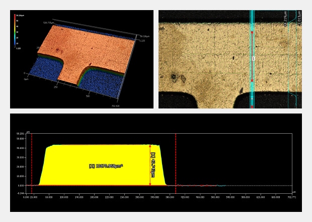
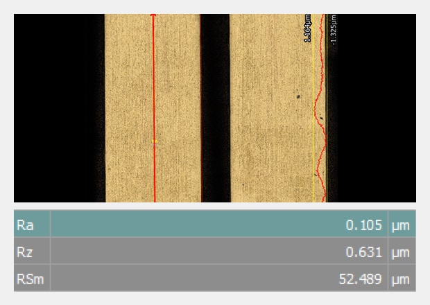
Pattern Gold-Plated Surface Roughness Inspection
Increasing the height display magnification allows users to emphasize subtle curvatures.
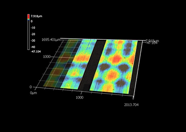
Height color image (100%)
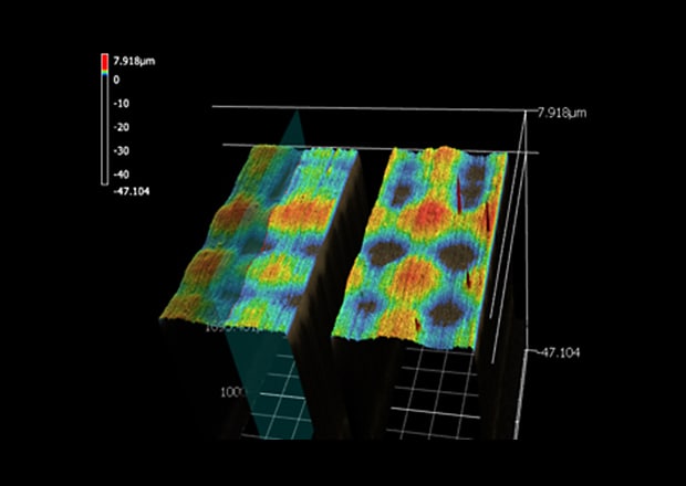
Height color image (4000%)
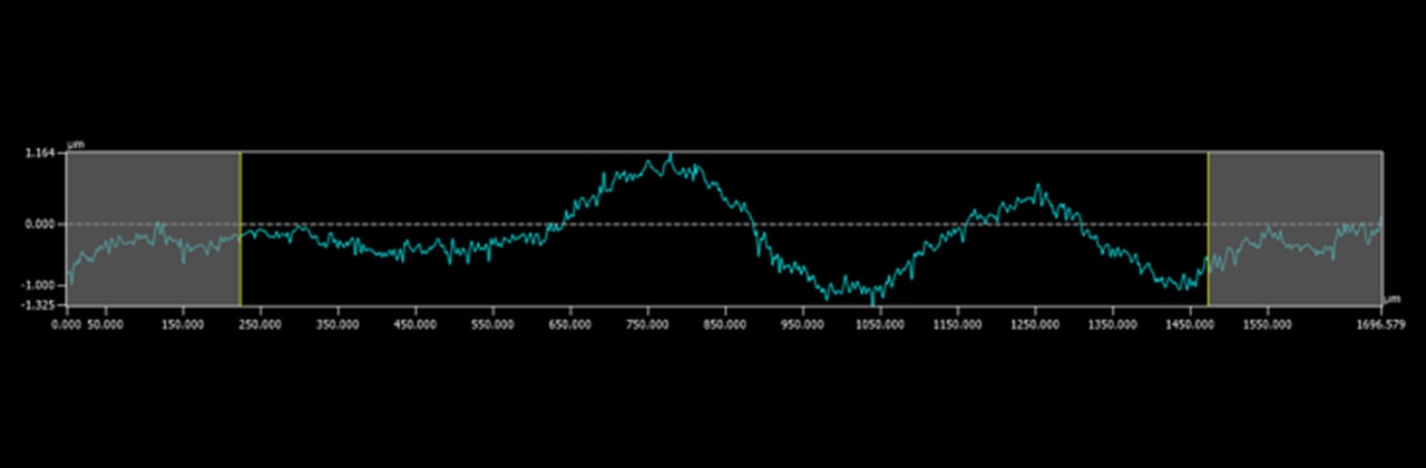
Cross-Sectional Measurement Curve
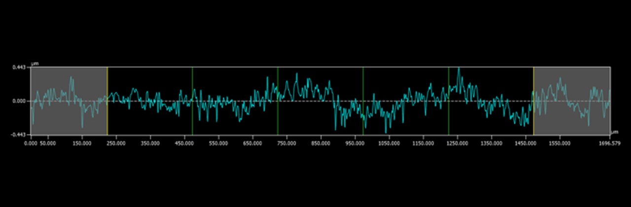
Roughness Curve

Basics of Soldering
What Is Soldering?
Soldering is a process used to join two different metals. An alloy is formed by tin in the melted solder and copper from the PCB.
What Does “Lead Free” Mean?
Conventional solder (eutectic solder/leaded solder) includes approximately 40% lead (tin 63%, lead 37%). The melting point is 183°C 361.4°F. Usually the solder is heated to approx. 250°C 482°F, but the burden placed on the environment by lead is large when it is disposed of as industrial waste. This has made lead-free solder more popular. The lead-free solder requires temperatures around 30°C 86°F higher and the wettability is inferior, so lead-free soldering is more difficult to perform.
What Is the Role of Flux?
Flux is used to increase the permeability and wettability of soldering. Rosin flux is commonly used and is effective for antioxidation during heating and the removal of oxide films and chemical stains.
Types of Solder
Thread Solder
Commonly used for soldering electronic components using a soldering iron. Thread solder has a tube shape with flux in the center.
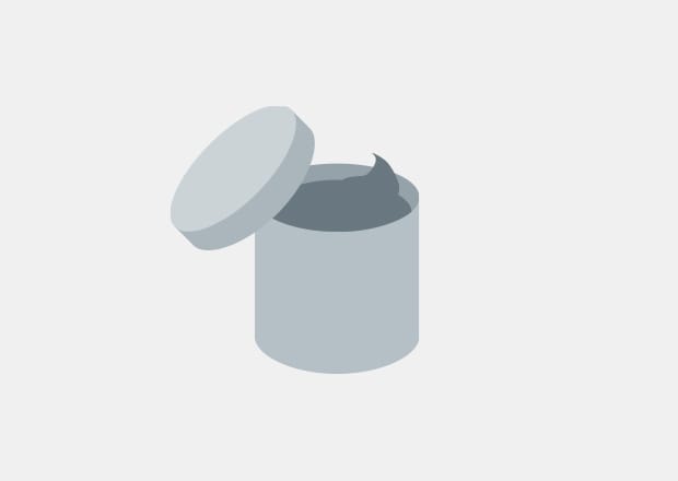
Cream Solder
Used for SMT, in which solder is printed on the lands of PCBs.
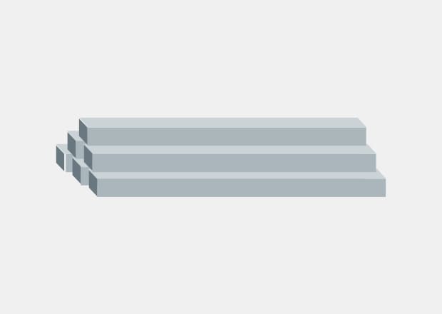
Solder Bar
Used for IMT, in which the terminals of parts and lands of PCBs are soldered in a soldering pot.
How to Solder
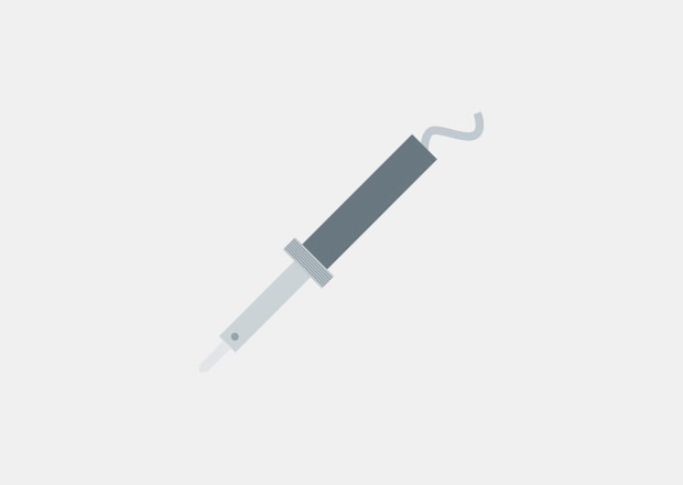
Soldering Iron
A tool used to heat solder and bonding points. Many irons are electric heaters that use nichrome wire or ceramic heaters. Using soldering irons with temperature control at the tip allows for more stable soldering.
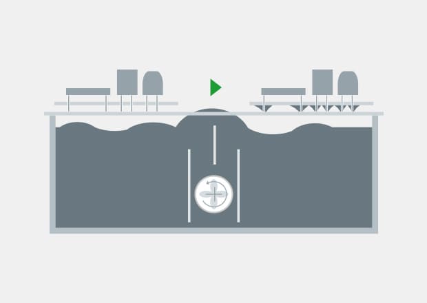
Flow Method
The bottom of the PCB is soaked in a soldering pot filled with melted solder. This is mainly used to mount lead-type DIP parts. There are 2 types of soldering pots: static soldering pots in which the melted solder surface is still, and wave soldering pots in which the surface is moving.
Reflow Method
Solder paste is printed on the PCB, and then heated to solder components. Reflow soldering is used to mount SMD components.
-
1Heat
PCB-Mounted Component Inspection Examples
Solder Fillet Inspection
The solder used to secure components is called the fillet.
Solder Volume and Cross-Sectional Area Inspection