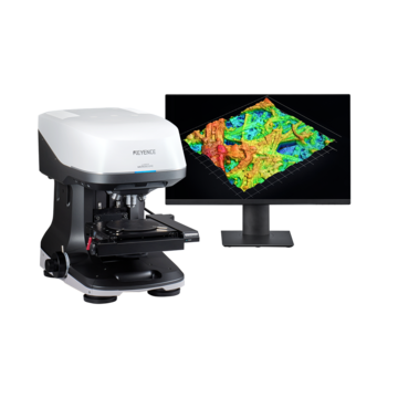
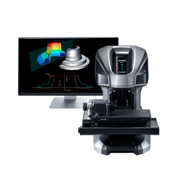
3D Optical Profiler: How to Choose the Right System
Key Takeaways
- A 3D optical profiler is a non-contact instrument that generates a complete three-dimensional map of a surface's topography without physically touching the part.
- Selecting the right optical profiler depends on vertical resolution, measurement range, surface type, speed requirements, and inspection environment.
- Non-contact 3D profiler solutions eliminate operator-dependent variation and remove the risk of marking or contaminating sensitive surfaces.
- The four main profiling technologies — white-light interferometry, confocal laser scanning, focus variation, and laser displacement — each perform differently depending on surface characteristics.
- Different industries require different profiling capabilities, from sub-nanometer semiconductor inspection to high-speed automotive surface analysis.
What Is a 3D Optical Profiler, and How Does It Work?
A 3D optical profiler is a non-contact measurement instrument that generates a three-dimensional map of a surface's topography to capture height, texture, roughness, flatness, and step features without physically touching the part. All optical profilers work on the same basic principle: light is projected onto a surface, and the reflected signal is analyzed to calculate height data across a two-dimensional measurement field. The result is a complete surface map acquired in a single pass, rather than a single-line profile.
This is what distinguishes 3D optical profilometers from a traditional contact-based stylus profilometers. A stylus probe drags a physical tip along one line of a surface, producing a cross-sectional profile of whatever it happens to traverse. An optical profiler captures the full surface simultaneously, revealing spatial patterns, directional texture, and localized features, such as scratches, pits, inclusions, and other defects, that a single-line trace would miss entirely unless it passed directly through them.
Where the different profiler types diverge is in their underlying measurement technology, each of which involves trade-offs in resolution, speed, measurement range, and surface compatibility.
| Technology | Working Principle | Best For | Vertical Resolution |
|---|---|---|---|
|
White-light interferometry
|
Working Principle
Analyzes interference patterns from broadband white light
|
Best For
Smooth, flat, or lightly textured surfaces
|
Vertical Resolution
Sub-nanometer
|
|
Confocal laser scanning
|
Working Principle
Uses a pinhole aperture to reject out-of-focus light
|
Best For
Steep slopes, rough surfaces, fine lateral detail
|
Vertical Resolution
Low nanometer range
|
|
Focus variation
|
Working Principle
Builds a height map from focus changes across a Z-stack of images
|
Best For
Complex geometries, high surface variation
|
Vertical Resolution
High nanometer to micrometer
|
|
Laser displacement profiling
|
Working Principle
Measures distance using a focused laser spot or line
|
Best For
Production environments, wide material range
|
Vertical Resolution
Low nanometer to micrometer
|
No single technology is universally superior. The right choice depends on the specific surface characteristics, resolution requirements, and operating environment of your application, which is a theme that runs through every aspect of profiler selection.
What Key Specifications Should You Evaluate?
Knowing what you need to measure and what those measurements need to tell you is the foundation of any profiler selection decision. Surface roughness, step height, flatness, and texture each place different demands on a profiling system, and starting with a clear set of measurement objectives will narrow your options considerably before you evaluate any specific features.
Vertical resolution is typically the first specification to examine. It defines the smallest height difference the system can reliably detect, which determines whether the profiler can capture the surface features that matter to your process. For applications such as semiconductor wafer inspection or optical coating measurement, nanometer to sub-nanometer resolution is a hard requirement since at those scales, even minor surface variations can affect device performance. General industrial inspection is more tolerant, but it is still worth confirming that a system meets your actual needs rather than assuming it does.
Measurement range must be evaluated alongside resolution, not in isolation. A surface that combines deep features with fine texture requires a profiler whose range and resolution are both appropriate for the full profile. A system optimized for high resolution at the expense of range will fail to capture the complete surface in a single pass, requiring multiple acquisitions or objective changes that slow down the process and introduce stitching complexity.
Field of view determines how much surface area is captured per measurement. A larger field of view accelerates inspection of bigger parts but typically reduces lateral resolution since the same sensor is covering more area. Systems with interchangeable objectives allow users to balance this trade-off based on the part being measured, which makes them more versatile across different applications.
Measurement speed should be matched to the profiler's role in your process before any other speed evaluation is done. A system that delivers results in seconds is well-suited to inline or near-line production inspection. One that takes several minutes per measurement may be entirely appropriate for a laboratory or R&D environment where thoroughness matters more than cycle time. The same specification looks very different depending on context.
Automation capabilities deserve careful consideration in any production setting. Systems that support motorized stages, automated measurement routines, and batch reporting reduce operator involvement while improving consistency. Software integration with quality management systems reduces manual data handling and simplifies traceability. Eliminating operator-dependent steps is one of the most direct ways to improve measurement reliability across shifts.
How Do Different Profiling Technologies Compare in Practice?
Understanding the four main profiler categories helps clarify which systems are likely to perform well in a given application and which may fall short in ways that a simple resolution figure won't reveal.
White-light interferometers achieve the highest vertical resolution of any common optical profiling technology, often reaching the sub-nanometer range. They perform best on smooth, flat, or lightly textured surfaces and are widely used in semiconductor manufacturing, precision optics, and applications where fine surface detail is critical. Their primary limitation is sensitivity to vibration, which can introduce measurement noise in production environments near heavy machinery, poorer lateral resolution when compared to other optical systems, and inability to collect data on steep slopes or highly-curved surfaces.
Industrial laser scanning confocal microscopes use a pinhole aperture to reject out-of-focus light, enabling reliable measurement of steep surface slopes and rough textures at high lateral resolution. They are particularly well-suited to applications where microscopic surface detail matters, such as tool wear analysis, structured surface inspection, and materials science research, where both imaging and dimensional data are needed from the same measurement.
Focus-variation systems build a height map by analyzing focus changes across a series of images captured at different heights. They handle significant surface variation well and work effectively on complex geometries, making them a strong choice for parts with pronounced texture or irregular form. Their flexibility across surface types makes them a practical option when a single system needs to handle a diverse range of parts.
Laser-based profilers combine measurement speed, ease of use, and robust performance across a wide range of materials and surface types. Their versatility makes them particularly well-suited to production environments, where the system needs to perform consistently without frequent manual reconfiguration between measurements.
What Industries Use 3D Optical Profiling, and Why?
3D optical profiling has become a standard measurement method across a wide range of industries, each with its own surface measurement requirements and performance targets.
Semiconductor manufacturing is among the most demanding application areas. Wafer surface inspection, nanoscale layer thickness verification, and defect detection all require resolution and repeatability that few other technologies can match. At semiconductor dimensions, surface imperfections invisible to any other inspection method can compromise device yield. Optical profilers are increasingly integrated directly into production workflows to enable real-time process control rather than after-the-fact inspection.
Automotive manufacturing presents a different set of challenges. Machined surfaces on engine components, sealing faces, and bearing and gear assemblies must meet tight surface finish specifications because texture directly affects wear rates, friction behavior, fluid sealing, and fatigue life. A surface that appears acceptable visually may still fall outside tolerance in ways that shorten part life or cause assembly failures. Optical profilers provide the quantitative, repeatable data needed to make confident pass/fail decisions in quality and manufacturing environments.
Medical device manufacturing relies on 3D optical profiling to verify implant surface finishes and confirm compliance with regulatory standards. Orthopedic implants, for example, often require precisely controlled surface textures to promote osseointegration or minimize wear in articulating joints. The non-contact nature of optical measurement is especially valuable here as it eliminates any risk of contaminating or altering a finished surface that has already passed prior inspection stages.
Electronics, aerospace, and precision tooling round out the industries where optical surface measurement has become routine. Solder joint inspection and PCB surface analysis benefit from the speed and repeatability of optical profiling. Aerospace applications such as coating thickness verification and fatigue-critical surface inspection demand both high resolution and comprehensive coverage. In precision tooling, wear measurement and edge geometry characterization support longer tool life and more consistent machining quality over time.
What Surfaces Can a 3D Optical Profiler Measure?
One of the most practical advantages of non-contact profiling is the breadth of materials it accommodates without surface preparation or any risk of damage.
Metals are the most frequently measured material in industrial contexts, including machined, polished, ground, coated, and anodized surfaces. Soft metals such as aluminum, copper, and gold are particularly well suited to optical profiling, since contact probes risk marking these surfaces even with careful force control. Plastics, ceramics, glass, and composite materials can all be measured effectively with standard equipment, and most produce clean, repeatable results without specialized settings.
Transparent and semi-transparent materials, including thin films, optical coatings, and certain polymers, require dedicated measurement modes to obtain accurate surface data. Without these modes, light penetrating the surface and reflecting from subsurface interfaces can corrupt the measurement signal and produce erroneous results. Modern optical profilers can typically measure both the film or coating thickness, as well as the topography on the surface or at film interfaces.
Highly reflective surfaces, such as polished metal and mirror-finish coatings, and strongly light-absorbing surfaces, such as black rubber or matte-coated components, can pose challenges for certain optical technologies. Contemporary systems address this through multi-exposure acquisition or adaptive measurement modes that automatically adjust to surface reflectivity. If reflective or absorptive materials are a regular part of your workload, confirming that a candidate system handles these conditions without manual intervention is a worthwhile step in the evaluation process.
How Does 3D Optical Profiling Compare to Contact-Based Measurement?
The limitations of stylus-based profiling become more consequential as measurement requirements become more demanding.
| Feature | 3D Optical Profiler | Contact Profilometer |
|---|---|---|
|
Measurement method
|
3D Optical Profiler
Non-contact optical
|
Contact Profilometer
Physical stylus contact
|
|
Data output
|
3D Optical Profiler
Full 3D surface map
|
Contact Profilometer
Single-line 2D profile
|
|
Surface risk
|
3D Optical Profiler
None
|
Contact Profilometer
Risk of marking or deforming soft or finished surfaces
|
|
Speed
|
3D Optical Profiler
Full-field acquisition in seconds
|
Contact Profilometer
Limited by stylus traverse rate
|
|
Probe wear
|
3D Optical Profiler
None
|
Contact Profilometer
Stylus tip degrades over time
|
|
Defect detection
|
3D Optical Profiler
Detects spatial patterns and localized features
|
Contact Profilometer
May miss features outside the trace path
|
|
Soft material suitability
|
3D Optical Profiler
High
|
Contact Profilometer
Low
|
A stylus profilometer physically contacts the surface at every measured point. This causes wear on the probe tip over time, risks marking soft or finished surfaces, and constrains measurement speed to the rate at which the probe can traverse a surface without losing contact. Because a stylus trace captures data along a single line, it produces a cross-sectional profile rather than a complete surface map, meaning any defect or feature that falls outside that line goes undetected.
Non-contact 3D optical profiling eliminates each of these constraints. The surface is left completely unaltered, which is critical for delicate parts, recently coated surfaces, and any component where visible marks are unacceptable. For surfaces in this category, non-contact measurement isn't simply more convenient, but rather it is often the only viable option.
What Challenges Arise in Industrial Optical Surface Measurement?
Even with the right system in place, some surface conditions and operating environments can still present challenges. It's worth thinking about these before deployment.
Reflective surfaces can saturate optical sensors and produce inaccurate or incomplete data. Systems with automatic exposure control or multi-exposure stitching address this by capturing multiple images at different exposure levels and combining them into a single, properly exposed result.
Large height variation is a common challenge on surfaces that combine deep grooves with fine texture. A profiler optimized for high vertical resolution at the expense of measurement range will fail to capture the full profile in a single pass. Evaluating range and resolution together, rather than treating them as independent specifications, ensures the system can handle the complete surface without requiring objective changes or measurement restarts.
Vibration sensitivity can introduce noise that distorts measurement data, particularly in interferometric systems. Profilers used near stamping presses, grinding equipment, or other vibration-generating machinery should include active or passive vibration isolation. Some systems are designed with production environments in mind and incorporate isolation as a standard feature; others are better suited to controlled laboratory conditions, and this distinction matters when selecting a system for a manufacturing floor.
Transparent or translucent materials present a different problem. Light penetrating the surface and reflecting from subsurface interfaces can interfere with the surface signal. Dedicated measurement modes designed for thin films and optical coatings eliminate this interference but confirming that a system includes these modes is necessary for applications involving coated or transparent parts.
Frequently Asked Questions
Q What is a 3D optical profiler used for?
A
A 3D optical profiler measures surface topography, such as roughness, flatness, step height, texture, etc., without contacting the surface. It is used in quality control, process development, failure analysis, and R&D across semiconductor, automotive, medical device, aerospace, and precision manufacturing industries.
Q What is the vertical resolution of a 3D optical profiler?
A
Vertical resolution ranges from sub-nanometer in high-end white-light interferometric systems to the low-nanometer or micrometer range in laser-based industrial profilers. Achievable resolution depends on the measurement technology, objective magnification, and operating conditions. Stated specifications should be verified under conditions that reflect actual measurement environments, not only ideal laboratory settings.
Q What is the difference between a confocal microscope and a white-light interferometer?
A
A laser scanning confocal microscope uses a pinhole aperture to reject out-of-focus light, excelling at steep slopes and rough surfaces with high lateral resolution. A white-light interferometer analyzes interference patterns to achieve superior vertical resolution and performs best on smooth, flat, or lightly textured surfaces. Both produce 3D surface maps, but they perform differently depending on surface characteristics. The right choice depends on the application.
Q Can a 3D optical profiler measure transparent surfaces?
A
Yes, with appropriate measurement modes. Standard profiling modes can produce errors on transparent or semi-transparent surfaces due to subsurface reflections. Specialized modes designed for thin films and optical coatings eliminate this interference and allow accurate surface measurement on these materials.
Q Which 3D optical profiler technology is best for semiconductor wafer inspection?
A
White-light interferometry and confocal laser scanning are the primary technologies for semiconductor wafer inspection. Both achieve the sub-nanometer vertical resolution required to detect nanoscale layer thickness variations and surface defects. The choice between them depends on surface roughness and the specific inspection parameters required.
Q What is the best 3D optical profiler for automotive parts inspection?
A
Laser-based profilers (good for production environments) and focus-variation systems are well-suited to automotive applications. Both offer high measurement speed and reliable performance on metallic surfaces, and both support automated measurement routines in some capacity.
Q What surfaces can a 3D optical profiler measure?
A
Most 3D optical profilers can measure metals, plastics, ceramics, glass, and composite materials. Reflective, dark, or transparent surfaces may require specific measurement modes, but modern systems increasingly handle these without additional preparation.
Q How does 3D optical profiling improve quality control?
A
Optical profilers replace operator-dependent manual inspection with automated, non-contact measurement, eliminating the variability introduced by different operators or equipment settings. They produce complete surface maps rather than single-line profiles, improving defect detection and enabling more reliable comparison against surface finish specifications. In many cases, a single optical profiler replaces multiple instruments, including those used for roughness measurement, step height verification, and visual inspection, into one faster, more consistent process.