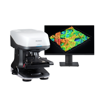
3D Optical Profilometry vs. AFM
Measurement Physics, Resolution Limits, and Application-Driven Selection
Abstract
3D optical profilometry and atomic force microscopy (AFM) both generate quantitative surface topography data, but their underlying physics impose fundamentally different resolution ceilings, throughput constraints, and measurable observables. This article compares the two techniques at a physical and instrumentation level. It covers measurement principles, noise floors, resolution limits, accessible data types, and application suitability to support instrument selection decisions in research and industrial metrology contexts.
Key Takeaways
- Optical profilometry is diffraction-limited in lateral resolution (approximately 130 nm for laser confocal; sub-micron for interferometry) but achieves sub-nanometer vertical resolution via phase or coherence detection.
- AFM lateral resolution is governed by tip radius (1-10 nm typical; below 0.1 nm in UHV), enabling imaging of individual molecules or atomic steps that no photon-based technique can reach.
- AFM scan areas are bounded by piezo actuator range and thermal drift, typically 100 micrometers x 100 micrometers or less. Optical systems routinely cover millimeter-scale fields, making them the only viable choice for macro-to-micro surface characterization.
- Tip-sample interaction forces in the pN to nN range make AFM sensitive to surface mechanics, adhesion, and electrostatics. These are observables that optical methods cannot access, but they also introduce potential sample perturbation.
- In industrial QC and process metrology, acquisition rate, calibration traceability, and operator burden favor optical profilometry for the large majority of applications.
Measurement Principles
3D Optical Profilometry
Optical profilometers encode surface height in the properties of returned light. Three dominant techniques each exploit different physical phenomena.
- Industrial confocal laser scanning microscopy (CLSM): uses a pinhole aperture to reject out-of-focus photons. Height is extracted from the intensity maximum as the focal plane is scanned axially through the sample. Lateral resolution is Rayleigh-limited: d = 0.61λ/NA, giving approximately 200-400 nm for a 405 nm laser at NA 0.95. Vertical resolution is determined by the confocal parameter and detection electronics, typically 10-50 nm in standard configurations.
- Scanning white-light interferometry (SWLI/CSI): measures optical path difference using broadband illumination. Coherence envelope detection yields height with sub-nanometer vertical precision (sigma-z below 0.1 nm with averaging) while remaining diffraction-limited laterally. SWLI is the ISO 25178 reference method for areal surface texture.
- Structured illumination and focus variation: project patterned light or exploit depth-of-field variation to extract height from contrast modulation. These approaches are practical for high-slope surfaces but typically offer lower z-precision than interferometry.
All optical methods share one fundamental constraint: they measure geometry, not interaction energy. They are insensitive to force, chemistry, and surface potential.
Atomic Force Microscopy (AFM)
AFM belongs to the scanning probe microscope (SPM) family. A microfabricated cantilever (spring constant k typically 0.01-40 N/m) terminates in a sharp tip with a radius of approximately 1-20 nm for standard silicon probes, or below 1 nm for carbon nanotube tips. As the tip approaches or contacts the surface, van der Waals, electrostatic, capillary, and Pauli repulsion forces deflect the cantilever. A laser-position-sensitive-detector (LPSD) system reads deflection with sub-Angstrom sensitivity. A feedback loop maintains a set-point deflection or oscillation amplitude while a piezoelectric XYZ scanner rasters the tip, producing a topographic map.
The three primary imaging modes differ in how the tip interacts with the surface.
- Contact mode: drags the tip across the surface under constant normal force. This produces the highest z-resolution but imposes significant lateral force on the sample, making it unsuitable for soft or loosely bound materials.
- Amplitude-modulated (tapping/AC) mode: drives the cantilever near its resonance frequency so the tip intermittently contacts the surface. Lateral shear forces are greatly reduced. Phase lag between drive and response encodes viscoelastic contrast.
- Non-contact (FM) mode: oscillates the tip above the surface without contact; frequency shift tracks long-range force gradients. This mode is required for true atomic resolution in UHV environments, for example NC-AFM imaging of Si(111)-7x7.
AFM lateral resolution is not diffraction-limited but tip-limited. For a hemispherical tip of radius R over a surface feature of height h, the apparent lateral broadening is approximately 2*sqrt(2Rh). In practice, this constrains usable lateral resolution to 5-20 nm on real surfaces with standard probes.
Quantitative Comparison
Table 1 summarizes the key metrology parameters across both techniques.
| Parameter | 3D Optical Profilometry | Atomic Force Microscopy (AFM) |
|---|---|---|
|
Measurement principle
|
3D Optical Profilometry
Reflected/scattered light (confocal, interferometric, structured illumination)
|
Atomic Force Microscopy (AFM)
Cantilever deflection via van der Waals, electrostatic, or contact forces
|
|
Lateral resolution
|
3D Optical Profilometry
Diffraction-limited; ~200-500 nm (confocal); sub-micron (interferometry)
|
Atomic Force Microscopy (AFM)
Tip-radius-limited; 1-10 nm typical; ~0.1 nm in UHV
|
|
Vertical (z) resolution
|
3D Optical Profilometry
~1-3 nm (interferometry); ~10-50 nm (confocal)
|
Atomic Force Microscopy (AFM)
0.01-0.1 nm; sub-Angstrom in contact mode
|
|
Max measurement area
|
3D Optical Profilometry
Millimeters to centimeters per field
|
Atomic Force Microscopy (AFM)
Typically 100 micrometers x 100 micrometers per scan
|
|
Acquisition speed
|
3D Optical Profilometry
Seconds per field; real-time at reduced z-resolution
|
Atomic Force Microscopy (AFM)
Minutes per scan (contact/tapping)
|
|
Contact with sample
|
3D Optical Profilometry
None
|
Atomic Force Microscopy (AFM)
Yes; tip-sample interaction forces in pN to nN range
|
|
Sample prep requirements
|
3D Optical Profilometry
Minimal; reflective or transmissive surfaces preferred
|
Atomic Force Microscopy (AFM)
Ultra-flat substrate; controlled vibration/humidity; no conductive coating needed
|
|
Measurement environment
|
3D Optical Profilometry
Ambient; liquid cell compatible
|
Atomic Force Microscopy (AFM)
Ambient, liquid cell, or UHV (UHV required for atomic resolution)
|
|
Accessible data types
|
3D Optical Profilometry
Height map, roughness (Sa, Sq, Sz), step height, film thickness (SWLI)
|
Atomic Force Microscopy (AFM)
Topography, force curves, phase contrast, mechanical properties (nanoindentation, adhesion)
|
|
Primary application domain
|
3D Optical Profilometry
Industrial QC, surface finish, thin film, MEMS inspection
|
Atomic Force Microscopy (AFM)
Nanomaterials, semiconductor R&D, biophysics, molecular imaging
|
Table 1. Side-by-side metrology parameters for 3D optical profilometry and AFM.
When Optical Profilometry Is the Appropriate Choice
Throughput-Constrained Applications
At the system level, AFM throughput is bounded by scan speed (above which piezoactuator resonance introduces image artifacts), cantilever Q-factor, and tip lifetime. Even high-speed AFM (hs-AFM) systems optimized for video-rate imaging operate on areas of tens of microns.
For process-line inspection of machined surfaces, thin films, or MEMS dies, millimeter-scale areas must be characterized across hundreds of parts per shift. In that context, optical profilometry is the only practically viable technique. A laser scanning confocal system can acquire a 5 x 5 mm area at sub-micron z-resolution in under 60 seconds; a comparable AFM scan would require hours.
Non-Contact Requirements for Sample Integrity
Tip-sample interaction in AFM is non-trivial even in tapping mode. Normal forces in tapping mode range from 0.1 to 10 nN, and the instantaneous contact stress during tip-sample impact can exceed the yield strength of soft polymers, hydrogels, and biological membranes.
Optical profilometry exerts zero mechanical load on the sample. For soft matter, live-cell surfaces, loosely adhered nanoparticle films, or low-modulus coatings, non-contact optical measurement preserves sample state in a way that contact-based techniques cannot guarantee.
Reflective and Transparent Materials
Metallic and mirror-polished surfaces are particularly well-suited for interferometric optical profilometry. Specular reflection maximizes fringe contrast and signal-to-noise ratio. Transparent films can be characterized for both surface topography and film thickness simultaneously using SWLI spectral analysis.
AFM performance does not depend on the optical properties of the sample, but the geometric complexity of polished metallic surfaces offers no practical advantage to probe-based methods either.
Complex Geometries and Re-Entrant Features
Industrial confocal systems with high-NA objectives can acquire surface data on steep slopes (up to approximately 85 degrees in some configurations) and inside recessed features via extended depth-of-field stitching.
AFM tips cannot access re-entrant geometries. Sidewall angles exceeding the tip cone half-angle produce artifactual broadening or complete loss of signal. For engineered surfaces with high-aspect-ratio features such as gear teeth, threading, and microchannels, optical measurement is geometrically superior.
When AFM Is the Appropriate Choice
AFM retains clear advantages in specific high-resolution research contexts. The four most common are listed below.
- Sub-diffraction lateral features: grain boundaries in 2D materials, DNA secondary structure, protein conformational states, and atomic step edges are not accessible to photon-based profilometry.
- Nanomechanical characterization: force-distance spectroscopy, PeakForce QNM, and conductive AFM (C-AFM) return Young's modulus maps, adhesion energy, and local conductivity alongside topography. No optical technique delivers equivalent multi-observable datasets from a single scan.
- Atmospheric and liquid environments at high resolution: liquid-cell AFM can image biomolecules under near-physiological conditions with nanometer lateral resolution, which is essential for structural biology and polymer science.
- Semiconductor process control at sub-10 nm nodes: line edge roughness (LER) and critical dimension (CD) measurements at technology nodes below 10 nm require AFM or CD-SEM. Optical systems are physically incapable of resolving these features.
Selection Framework
Decision Criteria
The choice between optical profilometry and AFM should be driven by the following hierarchy of constraints, evaluated in order.
- Required lateral resolution: if the critical feature dimension is below 200 nm laterally, AFM is likely required. If it is above 500 nm, optical profilometry is viable. The 200-500 nm range requires case-by-case evaluation.
- Measurement area: if the region of interest exceeds approximately 500 micrometers x 500 micrometers, optical profilometry is the only practical choice unless stitching is acceptable for the application timeline.
- Sample fragility and contact tolerance: contact mode AFM should not be used on any sample with modulus below 1 MPa without specific protocol development. Tapping mode extends the soft-material range, but optical methods remain the lowest-risk default.
- Observable type: if the application requires topography combined with mechanical, electrical, or chemical information from the same scan, AFM is the required platform.
- Throughput and operator skill: AFM requires trained operators for tip selection, spring constant calibration, and artifact recognition. Optical systems are substantially more accessible for routine QC workflows.
Metrology Standards Alignment
ISO 25178 (areal surface texture) is the dominant international standard for surface topography measurement in industrial metrology. It was developed primarily around optical instruments, including interferometry, confocal, and focus variation methods, and defines the filtering, parameter calculation, and calibration procedures used in manufacturing QC.
AFM is not typically used to generate ISO 25178 Sa/Sq/Sz parameters in production contexts. It is, however, used as a transfer standard for calibrating optical instruments at the sub-100 nm scale.
Frequently Asked Questions
Q What is the diffraction limit and how does it constrain optical profilometry?
A
The Rayleigh criterion sets the minimum resolvable lateral distance as d = 0.61*lambda/NA, where lambda is wavelength and NA is the numerical aperture of the objective. For visible light (400-700 nm) at practical NA values (0.7-0.95 for high-magnification objectives), this yields lateral resolution limits of approximately 250-600 nm. No optical profilometer can resolve two adjacent features separated by less than this distance, regardless of signal processing. AFM, being mechanical rather than photonic, is not subject to this constraint.
Q Is AFM more accurate than 3D optical profilometry for roughness measurement?
A
It depends on which roughness parameter and at what spatial frequency. AFM resolves high-frequency roughness components (short-wavelength features) that optical systems alias or average out due to their point spread function. For low-frequency components and average roughness (Sa) on typical engineering surfaces, calibrated SWLI systems provide results traceable to national length standards, with measurement uncertainty competitive with or superior to AFM in the 1 nm to 1 micrometer height range.
The relevant comparison metric is the power spectral density (PSD) function, which reveals the spatial frequencies at which each instrument's noise floor becomes limiting.
Q Can optical profilometry characterize nanoscale film thickness?
A
Yes. SWLI-based systems can extract film thickness for transparent or semi-transparent layers by analyzing the coherence envelope or spectral interference pattern. Thickness sensitivity extends to layers as thin as a few nanometers under optimized conditions, though accuracy depends on film refractive index, substrate reflectance, and surface roughness. This capability, providing film thickness and surface topography in a single non-contact scan, has no AFM equivalent.
Q What sample preparation does AFM require?
A
Less than SEM, but more than optical profilometry. AFM does not require conductive coatings or vacuum environments for standard imaging. It does require: (1) a substrate compatible with the measurement area, typically less than 100 mm diameter for standard stages; (2) mechanical vibration isolation, with active isolation tables needed for sub-nm work; (3) humidity control for hydrophilic or hygroscopic samples in ambient conditions; and (4) careful tip selection and force-curve validation to avoid measurement artifacts. The practical implication is significantly higher setup time and operator expertise per measurement compared to optical methods.
Q Is 3D optical profilometry limited by sample reflectance?
A
Low-reflectance or matte surfaces reduce signal intensity in interferometric modes and can push confocal systems below their detection threshold. Modern optical profilometers address this through variable illumination intensity, high-sensitivity detectors, and algorithms designed for low-coherence surfaces.
For most industrial materials, including metals, ceramics, polymers, and coatings, reflectance is sufficient. Truly transparent or anti-reflective samples such as bare glass or AR coatings may require adapted configurations. AFM has no reflectance dependency.
KEYENCE 3D optical profiling systems deliver fast, non-contact areal surface measurement with full ISO 25178 parameter output. Contact a KEYENCE applications engineer to discuss instrument selection for your specific measurement requirements.