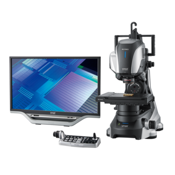
How Does a Scanning Electron Microscope Work?
Scanning electron microscopy (SEM) is an imaging technique that uses a focused beam of electrons to examine the surface of a sample at extremely high magnifications. As the electron beam scans across the specimen, interactions between the electrons and the sample generate signals that are used to create detailed images of surface structures and composition. Unlike optical microscopy, SEM provides exceptional resolution and depth of field, making it an essential tool for materials science, manufacturing, electronics, life sciences, and quality control. Understanding how scanning electron microscopy works helps researchers and engineers select the right imaging method for analyzing microscopic features and material properties.
Some materials hide their most interesting features at a scale no optical microscope can reach. That's where scanning electron microscopy comes in. Instead of visible light, it uses a focused beam of electrons to build images with a level of surface detail that's hard to match with other equipment. This guide breaks down what the technology actually does, piece by piece, so you can see why labs across so many industries rely on scanning electron microscopes.
Key Takeaways
- Scanning electron microscopy uses a focused electron beam to produce detailed images of a sample's surface.
- The imaging process involves generating electrons, scanning the sample, and detecting the signals they produce.
- SEMs reveal surface texture and material structure that optical microscopes simply can't capture.
- Industries from semiconductor to biomedical research rely on SEMs for inspection and failure analysis.
- Knowing how the technology works helps you decide when a SEM is the right tool for the job.
What Is Scanning Electron Microscopy?
Scanning electron microscopy is an imaging method that scans a sample's surface with a narrow beam of electrons rather than light. As the beam sweeps across the sample, it triggers a range of signals that a detector converts into an image. Because electrons have a much shorter wavelength than visible light, this approach delivers far higher magnification and resolution than any optical microscope.
Researchers first developed the technique in the mid-20th century, and it's since become a standard tool wherever surface detail actually matters, from failure analysis on a cracked bolt to inspecting the layers on a microchip.
How Does a Scanning Electron Microscope Work?
So, how does a scanning electron microscope work from start to finish? An electron gun at the top of the column fires a stream of electrons downward. Magnetic lenses focus that stream into a narrow beam and aim it at the sample, which sits inside a vacuum chamber. Scanning coils then sweep the beam back and forth across the surface in a grid pattern.. At each point, the beam knocks electrons and other signals loose from the sample.
Detectors pick those signals up and translate them into brightness values, which get assembled into the final image on screen. The whole process happens fast enough to produce a live, moving view of the sample as the operator adjusts focus or position.
The Key Components of a Scanning Electron Microscope
An SEM relies on several parts working together. The electron gun sits at the top and supplies the beam, usually via a heated filament or field-emission source. Below it, a column houses the magnetic lenses that shape and focus the beam as it travels downward. The vacuum chamber holds the sample and keeps stray air molecules from scattering the electrons before they arrive.
Detectors, often more than one type, capture different signals depending on what the operator wants to see, whether that's fine surface texture or compositional contrast. Finally, a computer system processes the incoming signal and displays it as a usable image, often alongside tools for measurement and analysis.
The SEM Imaging Process Explained
Breaking the process into stages makes it easier to follow how a raw electron beam turns into a finished image.
Electron Beam Generation
Everything starts at the electron gun, where a filament or emitter releases electrons that get accelerated by high voltage. Once the electrons leave the gun, they're accelerated by a voltage that typically ranges from a few hundred volts up to about 30 kV, depending on the setting used. A higher accelerating voltage gives the electrons more energy, which improves resolution but also causes the beam to penetrate deeper into the sample, something that matters when you're imaging delicate or non-conductive materials, since deep penetration can lead to charging or beam damage on samples that aren't coated. Condenser lenses, electromagnetic not light, then compress this stream into a fine, focused point, small enough to resolve tiny surface features once it reaches the sample.
Electron and Sample Interaction
When the beam hits the sample, several things happen at once. Some electrons bounce back as backscattered electrons, useful for showing contrast between different materials. Others knock loose secondary electrons from the surface itself, which are especially good at revealing fine topography. X-rays can also be released, and these get used for elemental analysis in systems equipped for it.
An SEM doesn't capture an entire field of view at once; instead, scanning coils sweep the focused electron beam back and forth across the sample in a raster pattern. As the beam strikes each point, it interacts with the sample's atoms and knock loose signals.
Image Detection and Formation
Detectors positioned around the chamber capture these signals as the beam scans point by point across the sample. Software then maps each signal's intensity to a corresponding pixel, building up the image line by line until the full picture appears. KEYENCE's SEM technology page covers more detail on how this detection process translates into sharp, usable images.
Advantages of Scanning Electron Microscopy
A SEM offers a few clear advantages over optical imaging. Magnification and resolution are both much higher, allowing users to spot features measured in nanometers rather than microns. Depth of field is another strength; SEM images stay in focus across uneven, three-dimensional surfaces in a way optical microscopes struggle to match.
Many systems can also pair imaging with elemental analysis, providing researchers with compositional data alongside the visual image. Together, these strengths make understanding how scanning electron microscopy works worthwhile for anyone who regularly deals with fine surface detail or material composition.
Common Applications of SEM
SEMs are used in a wide variety of industries. In materials science, it's used to study fracture surfaces, coatings, and grain structure. Semiconductor manufacturers rely on it to inspect circuit patterns and catch defects at scales optical tools can't reach. Biomedical researchers use SEMs to examine cell surfaces, tissue structure, and even bacteria.
Manufacturing and quality control teams turn to it for failure analysis, checking welds, and verifying that parts meet tight tolerances. KEYENCE's digital microscope lineup, including the VHX-X1 series, offers additional tools for teams that need fast, detailed imaging alongside their SEM work.
Ready to see how SEM technology can improve your inspection processes? Contact us today to discuss your application or request a product demonstration
Frequently Asked Questions
Q How does a scanning electron microscope work?
A
A SEM fires a focused beam of electrons at a sample, then detects the signals produced when those electrons interact with the surface, converting them into a detailed image and provides the material composition.
Q What are the main components of an SEM?
A
An electron gun, electromagnetic lenses, a vacuum chamber, detectors, and a computer system for processing and displaying the resulting image.
Q What are the advantages of scanning electron microscopy?
A
Higher magnification and resolution than optical microscopes, along with strong depth of field and the option to pair imaging with elemental analysis.
Q What industries use scanning electron microscopes?
A
Materials science, semiconductor manufacturing, biomedical research, and industrial quality control all rely on SEM for inspection and analysis work.