Sample Preparation for Electron Microscopes Complete Guide
Sample preparation for electron microscopes is a critical step that directly impacts image quality and analytical accuracy. Because electron microscopes operate differently than optical microscopes, specimens often require specialized preparation techniques such as cleaning, mounting, dehydration, conductive coating, or ultrathin sectioning depending on the imaging method. Preparation requirements are critical for scanning electron microscopy (SEM). Following proper sample preparation procedures helps minimize imaging artifacts, improves resolution, and ensures reliable results for research, quality control, materials science, and industrial inspection.
Good images start well before a sample ever reaches the microscope. Sample preparation for electron microscopes shapes everything that follows: how sharp the image looks, how much detail you can pull from it, and whether the results hold up to scrutiny.
Scanning electron microscopes (SEM) work differently than optical microscopes, so samples usually need extra preparation before they're ready for imaging. This guide walks through why sample prep matters, how it's done for SEM, and what tends to go wrong along the way.
Key Takeaways
- Proper sample preparation is essential for producing accurate, high-quality electron microscope images.
- Typical steps include cleaning, mounting, drying, coating, and sometimes sectioning, depending on the material.
- Rushed or careless prep can introduce artifacts that throw off both image quality and analysis.
- The right method depends on the sample itself, the microscope in use, and what you're trying to learn from it.
Why Sample Preparation Matters in Electron Microscopy
Electron microscopes form images using a beam of electrons instead of light, and that beam behaves in ways visible light never does. Electrons scatter off moisture, build up as static charge on non-conductive surfaces, and get absorbed by anything too thick to let them pass through. Skip proper prep, and you'll likely see charging artifacts, blurred edges, or a sample that degrades under the beam before you get a usable image.
Careful prep removes these obstacles ahead of time. It also protects the microscope itself, since a wet or unstable sample can contaminate the vacuum chamber and throw off imaging for the next user too.
How Are Samples Prepared for Electron Microscopes?
So, how are samples prepared for scanning electron microscopes? The process usually starts with cleaning to strip away dust, oils, or residue that would otherwise show up in the image. From there, the sample gets mounted onto a stub or grid, sized and shaped to fit the microscope's stage. Biological or wet samples often go through a dehydration step, since water doesn't survive the vacuum environment inside the chamber.
Many samples, particularly ones that don't conduct electricity, need a thin metal coating so the electron beam doesn't just pile up charge on the surface. SEM Sample Preparation Step by Step
SEM sample preparation generally follows three main stages, each one building on the last.
Cleaning and Drying the Sample
Before anything else, the sample needs to be free of contaminants. Technicians often use solvents, ultrasonic cleaning, or gentle rinsing to remove dust and oils without damaging delicate surfaces. Once clean, the sample has to be completely dry. Any leftover moisture will boil away inside the vacuum chamber, and that can distort the image or even damage the equipment.
Mounting the Sample
Next, the sample is fixed onto a metal stub, usually with conductive adhesive tape or conductive resin that also helps electrons flow off the sample rather than build up. Positioning matters here too. The angle and orientation you choose will affect which surface features show up clearly once imaging begins.
Conductive Coating Techniques
Many materials, especially ceramics and polymers, don't conduct electricity on their own. Left uncoated, they build up a charge under the electron beam that washes out the image. Sputter coating applies a thin layer of gold, platinum, or another conductive metal to solve this. Some labs use carbon coating instead, particularly when they also plan to run elemental analysis on the sample afterward. KEYENCE's SEM technology page covers more on how these systems capture surface detail once a sample is ready.
Common Sample Preparation Challenges
Even experienced technicians run into trouble here. Beam-sensitive materials, like certain polymers or soft tissue, can shrink, melt, or char under prolonged electron exposure. Charging remains a persistent issue too, especially when a coating layer turns out too thin or uneven. Samples with mixed composition, some conductive, some not, can be tricky to coat evenly, which sometimes leads to patchy or misleading results.
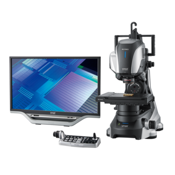
Tools like KEYENCE's VHX-X1 digital microscope can help teams check prep quality before committing a sample to a full SEM run, catching issues early instead of after the fact. The VHX digital microscope has many capabilities so teams may want to check if that microscope can solve their application before going through the sample preparation process for an SEM.
Frequently Asked Questions
Q Why is a conductive coating required for SEM?
A
Non-conductive samples build up static charge under the electron beam, which distorts the image. A thin conductive coating, often gold or carbon, allows that charge to dissipate, keeping the image clean. Many use a sputter coater to apply the thin layer of conductive coating.
Q What materials require special sample preparation?
A
Materials requiring special SEM prep generally fall into a few groups: non-conductive materials (polymers, ceramics, glass, biological tissue) need conductive coating (gold, gold-palladium, or carbon for EDS work) or low-vacuum imaging to prevent charging; hydrated or biological samples need fixation, dehydration, and critical point or freeze-drying (or cryo-SEM) so they survive high vacuum without collapsing; beam-sensitive materials need low voltage and minimal exposure to avoid damage; magnetic materials need careful mounting and shielding to avoid deflecting the beam; oily or volatile materials need degreasing to avoid contaminating the chamber; powders need thin, controlled dispersion on conductive tape; and samples where you need internal structure (metals, semiconductors, composites) need cross-sectioning, polishing, and sometimes etching or ion milling to get a clean, representative surface.
Q How can poor sample preparation affect imaging results?
A
Weak prep can introduce charging artifacts, blurred detail, or physical damage to the sample, all of which lower image quality and can lead to inaccurate analysis.
If you aren't able to or don't know how to properly prep your sample, take a look KEYENCE's VHX Series Digital microscope. This easy-to-use system is capable of magnification up to 6000x and can easily identify materials using LIBS.