Thin Film Thickness Measurement: The Essential Guide to Choosing the Right Method
Key Takeaways
- Match the method to the film. Reliable film thickness measurement depends on thickness range, transparency, substrate, surface roughness, and whether contact or sample damage is acceptable.
- Optical, non-contact methods lead for transparent films. Spectral interference suits sub-micron layers, laser confocal suits thicker layers and multilayer stacks, and ellipsometry suits few-nanometer films where optical constants are also needed.
- Opaque layers need a different approach. For these, coating thickness measurement usually means measuring step height at a masked or etched edge, or using X-ray or magnetic/eddy current methods on metal parts.
- Areal measurement reveals edge build-up and non-uniformity that single-point readings miss. Validate any method against a reference before trusting production data.
Film thickness rarely gets attention until something goes wrong. A few nanometers of drift in a dielectric layer shifts a device's electrical behavior. A few hundred nanometers of variation in an optical coating changes how much light it reflects. An uneven barrier or hard coat shows up as delamination, wear, or permeation failures.
The method that works perfectly on a 200 nm oxide can fail outright on a 20 µm polymer layer or a painted steel panel. That's why thin film thickness measurement is less about finding the best instrument than about finding the right one for the sample in front of you. This guide walks through the main ways to measure film thickness, explains why each works where it does, and shows how to choose between them and validate the result.
What Counts as a Thin Film?
There's no official cutoff. In industrial practice, "thin" usually means anything from a few nanometers to a few tens or hundreds of micrometers. Below about 1 µm, the top and bottom surfaces sit so close together that only interference- and polarization-based optical methods can tell them apart. Above that, confocal sensing, step-height profiling, and cross-sectioning become practical, and the distinction between a film and a coating starts to blur.
Multilayer stacks, rough or patterned substrates, and films with unknown optical properties can all complicate the picture. It's best to understand the sample before choosing the instrument.
What to Know Before Choosing a Method
Start with the film itself. The expected film thickness and the tolerance you need to resolve will rule out some techniques immediately. Transparency narrows the field further: optical methods need light to reach the lower interface and return, so opaque films call for a physical step, X-rays, or a cross-section instead. And because optical methods measure optical path length rather than physical film thickness, you'll need the film's refractive index to convert one into the other.
Next, look at what the film sits on: a silicon wafer, a glass panel, a polymer web, and a steel part each favor different techniques. Surface roughness weakens optical signals, and layer structure matters too, with some methods only reporting the total thickness of a stack, while others resolve each layer individually.
Finally, consider how you're allowed to measure. Soft polymers, wet films, and finished parts often rule out contact or cross-sectioning. If you need to monitor thickness dynamically, like in a deposition chamber, then that poses a different problem from inspecting a finished part.
The Main Film Thickness Measurement Methods
Each method below picks up where another leaves off, starting with the optical methods that are the default for transparent films.
Laser Confocal
As films get thicker, their surfaces move far enough apart for a confocal system to find each one directly. Laser confocal detects the precise focal position of every reflecting surface. On a transparent layer, it registers a peak at the top and another at each buried interface, and the distance between peaks, corrected for refractive index, gives thickness. Because every interface produces its own peak, confocal handles multilayer stacks as readily as single films, typically for transparent layers thicker than about 1 µm.
On opaque layers, it measures step height at a masked or etched edge, which makes it a practical route for coating thickness measurement on any part that can be prepared with a step. For these types of coatings, step height changes can be measured in the low nanometer range.
Spectral Interference
When a transparent film is too thin for focus-based methods to separate its surfaces, spectral interference reads them through reflected light. The two reflections (top surface and bottom surface) of broadband light interfere, creating a pattern of peaks and valleys across the spectrum. That pattern encodes the film's optical thickness, and dividing by the refractive index gives physical thickness.
That makes it the natural choice for clear coatings below 1 µm. The catch is that the film has to transmit light, and you have to know, or be able to determine, its refractive index. Using the VK-X4000's spectral interference mode, you can measure transparent films as thin as 0.1 um.
White Light Interferometry
When that step is only nanometers tall, white light interferometry (WLI) offers more vertical resolution. WLI scans an interference objective vertically and finds the height at which fringe contrast peaks for each pixel. Its resolution doesn't depend on magnification, making it strong for sub-nanometer step heights on very smooth surfaces.
Spectroscopic Ellipsometry
For films only a few nanometers thick, ellipsometry is the specialist. It measures how the film changes the polarization of light striking it at an oblique angle. Phase is so sensitive to very thin layers that ellipsometry can resolve films of a few nanometers and extract their optical constants (n and k) in the same measurement.
That sensitivity comes with a dependency. Ellipsometry fits a layer model to the data, and a wrong model can produce a convincing fit and a wrong answer. It remains the reference for ultrathin film thickness in semiconductor and materials R&D.
X-Ray Fluorescence and Reflectivity (XRF and XRR)
X-rays take over where visible light can't reach. XRF measures metallic layers, such as plating on connectors and PCBs, provided the calibration standards match the layer system. XRR works on very smooth stacks, resolving the thickness, density, and roughness of individual layers.
Stylus Profilometry and AFM
Sometimes the simplest approach is to touch the surface. Both stylus profilometry and AFM trace a physical step. The stylus is simple and traceable but can scratch soft films; AFM resolves nanometer-scale features over small areas. Both report only total stack thickness and cannot measure through a film like optical systems can.
Magnetic Induction and Eddy Current Gauges
On the factory floor, coatings on metal parts are usually checked with a handheld film thickness gauge. Magnetic induction works on ferrous substrates and eddy current on non-ferrous conductive ones, covering paint, powder coat, and anodize from a few micrometers to millimeters. They're fast and inexpensive but can't resolve sub-micron layers and won't work on glass, polymer, or silicon.
Cross-Section SEM and TEM
When doubt remains, cutting the sample open settles it. A cross-section shows every layer directly, down to individual atomic layers with TEM. Because it's destructive and slow, cross-sectioning serves as the reference for validation and failure analysis rather than as a routine check.
Method Comparison at a Glance
| Method | Typical range* | Contact | Film type | Best for |
|---|---|---|---|---|
|
Spectral interference
|
Typical range*
Sub-µm to tens of µm
|
Contact
Non-contact
|
Film type
Transparent
|
Best for
Clear coatings below 1 µm
|
|
Laser confocal
|
Typical range*
~1 µm and up (transparent); nm step height (opaque)
|
Contact
Non-contact
|
Film type
Transparent, multilayer, opaque via step
|
Best for
Thicker clear films, multilayers
|
|
White light interferometry
|
Typical range*
Sub-nm step heights and up
|
Contact
Non-contact
|
Film type
Any, with a step
|
Best for
Smooth surfaces, nanoscale steps
|
|
Ellipsometry
|
Typical range*
Sub-nm to a few µm
|
Contact
Non-contact
|
Film type
Transparent / semi-absorbing
|
Best for
Ultrathin films, n and k
|
|
XRF / XRR
|
Typical range*
~nm to tens of µm / ~1–500 nm
|
Contact
Non-contact
|
Film type
Metallic / smooth stacks
|
Best for
Plating; layer density
|
|
Stylus / AFM
|
Typical range*
nm to ~1 mm
|
Contact
Contact
|
Film type
Any, with a step
|
Best for
Lab verification
|
|
Magnetic / eddy current
|
Typical range*
~µm to mm
|
Contact
Contact
|
Film type
Coatings on metal
|
Best for
Paint, powder coat
|
|
Cross-section SEM/TEM
|
Typical range*
Atomic layers and up
|
Contact
Destructive
|
Film type
Any
|
Best for
Reference, failure analysis
|
*Typical values. Ranges vary by instrument.
How to Choose: A Practical Decision Path
You should start with the type of film that needs to be measured. If light can't pass through the film, the material points the way: XRF for plating on metal, a magnetic or eddy current gauge for paint or powder coat on metal, and for anything else, a step-height measurement by confocal or WLI, or a cross-section.
If the film is transparent, film thickness decides. For a few nanometers, or when you also need n and k, ellipsometry is the tool. Below 1 µm, spectral interference fits best. Above about 1 µm, or when there are multiple layers, laser confocal takes over.
Rough surfaces favor confocal, and small or patterned features call for a method that can target a precise location. And if uniformity matters, a single reading won't tell you enough; you need a method that maps thickness across the part.
How to Validate Your Results
Clean off oils and fingerprints from the sample without altering the film, and keep a witness coupon from the same deposition run for cases where the actual part can't be sectioned.
Then get the material data right. For interference-based methods, thickness scales inversely with refractive index, so a 2% error in n becomes roughly a 2% error in film thickness. Confirm n for your actual material and process. The same logic applies to calibration references. One with the wrong coating-substrate pairing, such as nickel on steel when you're measuring nickel on copper, will bias every result.
Don't trust a single spot - measure multiple locations, including edges, where build-up and thinning are most common. When a reading is borderline or critical, confirm it with a second method, typically cross-section or ellipsometry, and report the uncertainty alongside the thickness value.
Measuring Film Thickness with a 3D Optical Profiling Microscope
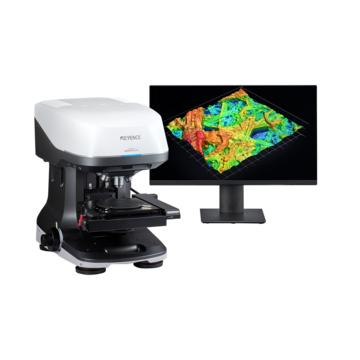
The decision path shows that the right method often changes from sample to sample. KEYENCE's VK-X4000 series 3D optical profiling microscope takes a different approach, combining laser confocal, white light interferometry, focus variation, and spectral interference in a single system.
With the VK-X4100 measurement head (404 nm laser), that coverage spans the full range of transparent films. For sub-micron clear coatings, the VK-T300 spectral film thickness unit uses spectral interference to measure films as thin as 0.1 µm, with repeatability (σ) of 0.1 nm and accuracy of ±0.6% (typical values under the default measurement environment). Once a film passes about 1 µm, laser confocal measures through it, including stacks of multiple layers. For opaque coatings, laser confocal and WLI measure step height at masked or etched edges, along with surface roughness.
Film thickness can be measured at a precisely specified spot, such as a single feature on a patterned or uneven surface. And when the refractive index is the weak link, a Material Search function compares the measurement against a material database and identifies the most likely coating or substrate material.
Ellipsometry still leads for few-nanometer films where optical constants are needed, and handheld gauges remain the fastest choice for paint on steel. But for labs and QA teams that need to measure film thickness across many sample types, one system covering four principles means fewer instruments to buy, maintain, and train on.
Start With the Film, Not the Instrument
What the film is made of, how thick it is, what it sits on, and how the results will be used determine which technique will give a trustworthy answer. Answer those questions, validate against a reference, and get the material data right, and choosing a film thickness measurement method becomes straightforward. To see how the VK-X4000 handles your film thickness samples, request a demo or sample test with a KEYENCE application engineer.
Frequently Asked Questions
Q What is the most accurate method for film thickness measurement?
A
It depends on the film. Ellipsometry offers the highest sensitivity for few-nanometer transparent layers. Spectral interference delivers sub-nanometer repeatability on sub-micron clear coatings. Cross-section SEM or TEM is the usual reference for physical verification.
Q Can thin films be measured without contacting the sample?
A
Yes. Spectral interference, laser confocal, white light interferometry, ellipsometry, and X-ray methods are all non-contact.
Q How are multilayer films measured?
A
Laser confocal resolves each interface in transparent stacks with layers thicker than about 1 µm. Ellipsometry and XRR resolve thin stacks when an accurate layer model is available. Cross-sectioning verifies each layer's film thickness directly.
Q Can a handheld coating gauge measure thin films?
A
Generally not below about 1 µm, and not on non-metallic substrates such as glass, polymer, or silicon.
Q What if I don't know the film's refractive index?
A
Determine it with ellipsometry, use supplier data for the specific material and process, or use a system with a material database that identifies the most likely material. An assumed index is a common source of optical thickness error.
Q How does coating thickness measurement differ from thin film measurement?
A
Coating work usually involves opaque protective or functional layers on parts, measured by step height, magnetic, eddy current, or XRF methods. Thin film work usually involves transparent layers on wafers, glass, or polymer, measured optically.