Measurement Sensors
Dimension Measurement
Displacement Measurement
Printed Circuit Board Inspection for Flawless PCB Quality
The complexity of today’s printed circuit boards (PCBs), with their dense layouts and multi-layer designs, has to be thoroughly inspected at every stage of production. If a single flaw or error is missed, even small ones, it can lead to costly hardware failures. With advanced printed circuit board inspection techniques manufacturers can ensure the quality of their PCBs and maintain customer trust.
Get detailed information on our products by downloading our catalog.
View Catalog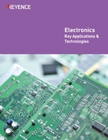

Why Printed Circuit Board Inspection is Essential
PCB inspections are important as they ensure the functionality, reliability, and longevity of electronic devices. As these components become more complex in their designs, the smallest of defects can lead to system failures that disrupt operations or, in the worst case, endanger lives. This is especially true in the automotive and healthcare technology industries where safety and precision are the difference between life and death.
When a manufacturer skips or poorly inspects a PCB, they risk delivering products that fall short of quality expectations. Defects like solder bridges or misaligned components can lead to product malfunctions and customer dissatisfaction. Failures can also erode a company’s reputation and destroy customer trust, which can be detrimental to anyone in the competitive electronics market.
Inspections aren’t just about identifying issues either. They add a proactive quality control process to save time and cost. If a manufacturer can address a problem before assembly progresses, they can reduce waste and avoid rework while keeping everything on a tight production schedule. Furthermore, consistent inspections allow for continuous improvement. Whether through identifying recurring defects or refining processes, inspections elevate the overall quality of PCBs.
Advanced PCB Inspection Methods for Flaw Detection
Traditional inspection methods, like manual visual checks, have long served as the first line of defense against PCB defects. While these methods are effective for simply designed components, they struggle with the overall complexity of modern PCBs. Thankfully, advanced methods have emerged to help detect flaws with precision and efficiency, thus ensuring that every PCB inspection is done correctly.
One method is called the Automated Optical Inspection (AOI). AOIs use high-resolution cameras and strategic lighting to identify surface-level defects. They are very useful in identifying issues like solder bridges and misaligned components. AOI systems also offer 2D and 3D capabilities. 2D focuses on surface analysis whereas 3D uses depth measurements.
Another inspection process is the X-ray inspection method which helps identify defects that are hidden to the naked eye. By using the penetrative properties of X-rays, inspectors can uncover concealed joints, voids, and cracks in densely packed or multi-layered PCBs. Advanced techniques such as 2D, 3D (oblique view), and computed tomography (CT) measurements can provide very exact details of a PCB. CT scans in particular offer a comprehensive 360-degree view of a board’s internal structure regardless of complexity. This allows an inspector to see within the component without having to take it apart.
Thermal imaging is another inspection technology that is used for one specific purpose: heat. By using infrared cameras, thermal imaging can detect abnormal temperature distributions across a PCB. This technique is especially valuable in pinpointing defects that occur under different operating conditions.
We’re here to provide you with more details.
Reach out today!

PCB Defect Inspection
PCB inspection serves as the primary defense against a wide range of defects that can compromise electronic devices. Issues like cold solder joints, insufficient solder, and copper trace damage, as well as cracks and contamination can all degrade performance.
Visual inspections provide a baseline for detecting surface damages, while advanced methods undercover the more hidden and complex flaws. Integrating AOI and X-ray technologies throughout the production cycle can help minimize defects; it also helps enhance reliability and optimize quality. On top of that, in-circuit testing (ICT) testing can measure the electrical properties of each component and help simulate real-world conditions to identify potential failures before deployment.
If you’re looking to ensure flawless PCB quality with advanced inspection solutions designed to detect defects and optimize production, look no further. KEYENCE has over 50 years of experience and we're here to take care of you and your needs. Our cutting-edge technologies offer accuracy and reliability to empower you to meet the demands of modern electronics manufacturing. Explore KEYENCE’s quality assurance solutions today and elevate your production processes to new heights.
Contact us to learn more about how our advanced technology can help take your business to the next level.
Contact Us
Related Products
Applications
Dimension Measurement
- Thickness and Width Measurement
- Step Height Measurement
- Inner and Outer Diameter Measurement
- Measuring Angles
- Meandering/Edge Measurement
Displacement Measurement
- Positioning and Stroke Length Measurement
- Vibration and Runout Measurement
- Deflection Measurement
- Measuring Eccentricity

