Industrial Laser Marking Systems / Laser Markers
Which Type of Lasers Are Used in Semiconductor Manufacturing?
-
Tags:
- Semiconductor , Laser Cutting , Laser Labeling
Semiconductors are a critical component of electronic devices—whether it’s a phone, electric vehicle, or computer, semiconductors are an integral part of the inner workings. Semiconductors assist the conductivity between a non-conductor and a conductor and, in turn, control the electricity flow.
The assembly process is extremely detailed, with many steps to create the perfect semiconductor that is the foundation of so many electronics. Although semiconductors are complex to manufacture, using semiconductor laser equipment makes manufacturing more tolerable.
Several types of semiconductor lasers are used in semiconductor manufacturing. These lasers are built to serve unique purposes and feature a broad range of capabilities and use cases.
Some of the most common semiconductor lasers include:
- CO₂ lasers
- UV laser markers
- Solid-state lasers
The whole of semiconductor laser technology is more complex than a simple approach to the manufacturing process. This same sentiment applies to laser marking methods, as there is a long list of technologies included with the term.
Laser technology is frequently used in semiconductor manufacturing because of its thin, precise, versatile, and powerful beam. Using lasers for manufacturing is effective and has been successful with cutting, marking, coating removal, measuring, and welding. In this article, we’ll discuss the fundamentals of semiconductor lasers, the types of lasers used, their applications, the manufacturing process, and the future of lasers.
Wafers
Silicon
Crystal Oscillators
Nickel plating
Lead Frames
Copper
IC Packages
Epoxy
Main Types of Lasers Used in Semiconductor Manufacturing
Solid State Laser
Solid state lasers are the most frequently used lasers for manufacturing. These lasers are a category of lasers known for high power and their use of ores for the laser medium. The ores are commonly made up of yttrium, aluminum, garnet, or yttrium vanadate crystal. The machine oscillates light through the medium in order to refine the wavelength and output a clean, concise beam.
Fiber Laser
Fiber lasers are a type of laser within the solid-state category. These lasers are known for high-speed marking, engraving, and cutting. A fiber laser uses fiber as a resonator and creates an overlapping structure with fiber cladding doped with Yb ions. After that, it pumps the laser diode excitation inside for use. Some uses for fiber lasers include removing burr in the preproduction process, marking traceability codes, and removing resin to analyze defects. KEYENCE’s fiber laser is called the MD-F Series 3-Axis Fiber Laser.
Excimer Laser
Excimer lasers are deep ultraviolet lasers with a 126 nm to 351 nm wavelength. These semiconductor lasers are used for polymer micro-processing.

Laser Technology and Its Role in Semiconductor Manufacturing
Cutting
Semiconductors go through a long production process that includes various cutting steps. For instance, semiconductors are made from cutting out wafers from crystal blocks and cutting stencils out of films.
Because of the high-powered laser with a thin beam, lasers are used for the ability to cut cleanly. Clean cuts are necessary as semiconductors have to fit nicely into the final product, like a phone, computer, or camera.
Welding
Semiconductor (LD) laser welding, also known as laser diode welding, is the process of melting adjoined sections together. This type of laser welding is special because it does not use a lamp as the excitation source. One example of adjoining in semiconductor manufacturing is welding a wafer to a supporting plate.
Removing Coating
Coating removal for semiconductors is part of the manufacturing process for cleaning the semiconductor or analyzing defects. Removing coating could be deburring resin or copper, removing gold plating, or removing thin film coating. In the instance of deburring, semiconductor lasers use their thin and precise beam to remove excess material without damaging any of the product.
On the other hand, removing coating for analyzing a defective mold also allows manufacturers to see a defect without disassembling and damaging the product.
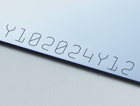
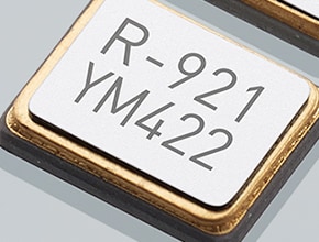
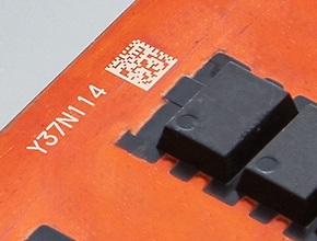
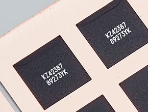
Marking
Laser marking machines are used for 2D code marking on IC chips, LED ceramic packaging, silicon wafers, and more. Since the laser marker has an extremely small beam spot, the laser can create readable marks even at microscopic levels.
Measuring
Laser sensors can measure semiconductors at many different steps of the semiconductor fabrication process. With wafers, KEYENCE’s LT-Series laser sensor measures thickness, wear level, and thermal expansion. Sensors can also measure wire bonding height, the height of resin molds, and the shape of BGA balls.

Applications of Laser Marking in Semiconductor Manufacturing
As multifaceted tools, laser markers are another key component of semiconductor laser instruments. From wafer identification to package marking and even trimming materials, lasers can be very adaptable across applications. The brief sections below offer insight into some of the most common applications of laser marking in semiconductor manufacturing.
- Wafer ID: Semiconductor lasers are commonly used for identification purposes. Regarding this manufacturing process, it is used for wafer IDs, serial numbers, and other types of ID codes. This is put in place to ensure traceability from one part to the next.
- Dicing Marking: Another application of semiconductor lasers is dicing marking. To ensure precision when separating wafer chips, a fiber laser engraver or other head design cuts scribe marks into the surface of the wafer. A dicing saw then uses these lines as a reference point to ensure efficient part separation while simultaneously mitigating waste.
Regulatory Requirements and Safety Considerations Related to Laser Marking in Semiconductor Manufacturing
As with any form of manufacturing, regulations and safety are vital considerations alongside semiconductor lasers. Starting with compliance, these requirements can pertain to standards from organizations like OSHA or the IEC.
It should be highlighted that regulations can easily shift based on changing laws, the consumer's location, and many other factors. Aside from this focal point, internal safety measures are paramount across the board. For instance, PPE gear and laser safety protocols should be consistently employed when it comes to the use of semiconductor lasers.
Other notable safety factors include:
- Meeting any labeling requirements by law
- Ensuring material safety
- Controlling gas emissions from laser technology
You can never go too far with safety, and following regulations guarantees manufacturing processes can continue from one day to the next.
Quality Control and Assurance in Semiconductor Laser Technology
When using semiconductor lasers in manufacturing, many aspects are susceptible to error, so proper quality control procedures must be in place at all times. Multi-step quality control processes help guarantee consistency with every part, some of which comes down to the technology used.
The precision and consistency that hybrid laser markers and other laser designs are capable of only help improve quality control outcomes. With fewer human errors and mechanical inconsistencies in the mix, manufacturers, consumers, and everyone in between benefit from its use.
Detailed reporting, traceability, and material selection are all core characteristics of laser marking technology, and this shows in quality control processes.
Weighing the Benefits and Obstacles of Laser Ablation in Semiconductor Production
Benefits of Laser Ablation
- Efficient
-
Lasers use automation and repeated tasks to conduct processing. The only hands-on step involves programming the laser for the application that is needed.
- Versatile
-
Because excimer lasers have high absorption rates and thin beams, laser ablation can be done on a wide range of materials.
- Precise
-
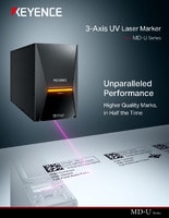
With the power and thin beam combined, excimer lasers are precise when conducting ablation. For instance, KEYENCE’s lasers include 3-axis control that autofocuses and autocorrects based on the target area for uniformity across the whole material.
Disadvantages
- High Initial Cost
-
Laser machines are an investment with a high initial cost; however, the benefits of precision and versatility often provide a great ROI.
A Step-by-Step Overview of Laser-Based Semiconductor Fabrication
Here’s an example of the step-by-step process of the semiconductor fabrication of an IC package:
1. Materials Are Purified and Shaped into Wafers
Wafers are the raw material used for starting fabrication. Lasers have many roles with wafers including, cutting wafers out of an ingot, dicing after lamination, marking identifiers for "good" or "no good", and marking 2D codes.
2. Bonding to Lead Frames
After the wafers are cut out by lasers, they are bonded to lead frames. For the lead frame to be ready for the wafer, the laser will mark the frame with an identifying mark. After that, laser markers roughen the surface for the lead frame and wafer adhesion. Once they are stuck together, the laser marker removes the burrs. Finally, when the burrs are removed, the laser marker once again marks the frame.
3. Molding and Processing
Now that the lead frame is done, it is ready for molding and processing to turn into an IC package. When the IC package is made, the laser once again marks identification on both the wafer and package.
Past, Present, and Future of Laser Applications in Semiconductor Manufacturing
Semiconductor lasers have been around for over 60 years and have evolved greatly over time. Beginning with a single wavelength without a clear purpose, lasers are now a multi-faceted and popular technology that assists across the semiconductor manufacturing process. Lasers measure, cut, clean, mark, and weld semiconductors, and there is only more innovation to come.
As semiconductors develop and new technologies arise, laser applications will face new opportunities to show off the technology. Looking to the future, it’s predicted that lasers will only get stronger in power and shorter in pulse for more efficient manufacturing.
![Laser Marker Installation Examples [Electronic Device Industry]](/img/asset/AS_117224_L.jpg)