Measurement Sensors
IC (Integrated Circuit) Cosmetic Defects Detection
Manufacturers of integrated circuits rely on precision at every stage of production as even small cosmetic defects can indicate deeper structural flaws, leading to product failures, electrical inconsistencies, or costly rework. With the demand from consumer electronics to automotive applications growing, manufacturers are looking for ways to implement high-precision inspection methods for integrated circuits in order to maintain quality and reduce waste.
Get detailed information on our products by downloading our catalog.
View Catalog

The Importance of Cosmetic Defect Detection in Integrated Circuits
Defects can develop at any time, during wafer fabrication, packaging, or handling, which makes early detection important to the final product. While some irregularities are purely cosmetic, others can compromise reliability. While manual inspections are prone to human error, automated inspection systems eliminate the subjectivity of manual checks, identifying surface irregularities before they affect circuit functionality.
Why Cosmetic Defects Impact IC Performance and Reliability
Surface defects in integrated circuits are more than just visual imperfections; scratches, voids, and delaminations can disrupt signal integrity, introduce stress points, or lead to long-term degradation. These issues often result from mechanical stress, contamination, or material inconsistencies during manufacturing.
Failure to detect and address these defects early can lead to increased electrical resistance, weakened encapsulation, and higher rejection rates, each of which contributes to production inefficiencies and unnecessary costs. Reliable defect detection supports higher yield rates, minimizes material waste, and maintains consistent quality across production batches.
Common Cosmetic Defects in Integrated Circuits
A wide range of defects can impact integrated circuit defects and overall quality; cosmetic defects take many forms, often originating from handling errors, fabrication inconsistencies, or environmental exposure.
- Surface scratches and scuffs from material handling may disrupt signal transmission, affecting circuit performance.
- Delamination, where layers within the circuit package separate, increases vulnerability to moisture damage and electrical failure.
- Voids and air gaps may be nearly invisible but compromise structural integrity.
- Burrs and uneven edges, formed during cutting or molding, can affect connectivity and assembly precision.
- Contamination from particulates, oxidation, or chemical residue introduces reliability risks that may go unnoticed without high-resolution inspection.
Many of these defects evade manual inspection methods which reinforces the need for automated, high-precision surface measurement systems that make sure defects are identified early in the production process.
Advanced Inspection Methods for IC Defect Detection
Traditional defect detection methods often struggle with low-contrast defect irregularities that are only visible under specific lighting conditions as they rely on visual inspection, standard imaging techniques, or rule-based algorithms. Standard imaging techniques often lack the resolution to identify micro-defects, and rule-based vision systems fail when defect variations extend beyond pre-programmed parameters. Manual inspection introduces inconsistency, as detection quality depends on the skill and focus of an operator.
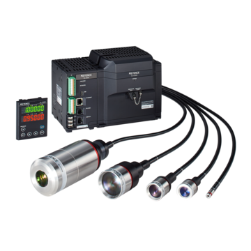
High-speed automated inspection systems have transformed integrated circuit defect detection by eliminating human error, detecting sub-micron defects with greater accuracy, and reducing false positives that lead to unnecessary rejections. Laser measurement technologies offer a superior alternative by providing non-contact, real-time surface analysis as systems quickly detect and classify systematic defects in integrated circuits, allowing manufacturers to improve quality control without slowing down production.
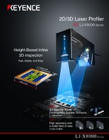
Laser Profiling for High-Precision Inspection
Laser measurement solutions offer unmatched precision for integrated circuit defect detection by scanning surfaces at high resolution. Unlike traditional imaging techniques, laser profiling provides real-time 3D surface mapping which identifies defects that might have been missed otherwise.
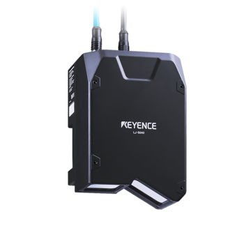
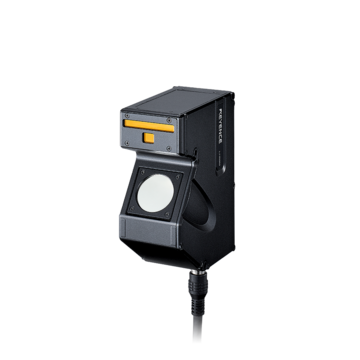
KEYENCE’s 2D laser and 1D laser technologies provide accurate and repeatable defect detection across a variety of semiconductor applications by delivering consistent real-time analysis. With semiconductor inspection solutions designed for precision, manufacturers can improve quality assurance and reduce waste with confidence. KEYENCE’s measurement technology helps manufacturers prevent defects from reaching the next stage of production.
Enhance IC Quality: Optimize Your Defect Detection Process Today!
Cosmetic defects in integrated circuits impact functionality and reliability, as well as production efficiency. Fortunately, KEYENCE’s industry-leading solutions help manufacturers identify flaws, reduce waste, and maintain optimal product quality.
With KEYENCE, you can boost your manufacturing process and meet rigorous industry standards. Improve your quality control and keep your integrated circuits defect-free with our advanced technology that integrates seamlessly into your production line.
Discover how KEYENCE's high-precision measurement technology can upgrade your inspection process and help you achieve higher yield rates. Measure with confidence, contact us today to learn more about how you can improve your defect detection and your bottom line.