Measurement Sensors
4 Effective Methods for Surface Deformation Inspection

Surface deformation - whether it's a crack, dent, or subtle inconsistency - can jeopardize the safety and longevity of a product. From the smooth glide of a car door to the precise fit of a smartphone screen, surface deformation can cause huge problems. These flaws may be structural or aesthetic. Regardless, they can lead to equipment failure and customer dissatisfaction.
Advancements in surface inspection technologies have reformed the way manufacturers detect and address deformation. Modern systems use techniques like AI-powered automation, optical surface inspection, and 3D imaging to execute surface inspections with enhanced accuracy and speed.
Selection of the right method for deformation inspection depends almost entirely on the industry and materials involved. Electronics manufacturing, with its need for microscopic precision in identifying defects on circuit boards and semiconductor wafers, has different needs than the automotive industry where the inspection takes place over a much broader surface area.
Why Surface Inspection is Crucial in Quality Control
Surface inspection is the last line of defense in quality control. It helps ensure that every product meets its standard before it goes out to customers. Industry leaders are tasked with the guarantee that their products are reliable– else face the consequences. For example, imagine a hairline crack in an airplane wing or a microscopic imperfection in a semiconductor chip. These tiny flaws, if undetected, can lead to significant product failures and safety hazards. In some instances, they can result in catastrophic events.
Every defect caught early is a problem avoided later. Modern surface inspection systems can identify issues in real time, which prevents the defective product from advancing through the production process. This proactive approach reduces waste and lowers production costs. For manufacturers, surface inspection isn’t just about catching flaws. It's also about creating a streamlined and efficient production cycle that minimizes downtime and rework.
Surface defects that compromise appearance, let alone functionality, can impact a company’s reputation. Customers are hesitant to buy products that have visible wear, even if it was from the production of the product; a scratch or crack is a risk customer do not want to take. Surface defect inspections make sure that every product adheres to their regulatory requirements and aligns with customer expectations.
Ultimately, surface inspections help build trust between manufacturers and their customers. While finding flaws is a part of the process, it’s more about reinforcing quality at every step in the process.
Key Methods for Optical Surface Inspection
Surface inspection methods have evolved over the years, with optical techniques offering precision and reliability you simply can’t replicate with other methods. From basic visual checks to more advanced imaging technologies, each of the following methods has a distinct role in identifying and addressing surface defects.
Visual Inspection Techniques
This method is one of the most fundamental methods for surface assessment. Manual inspections, often aided by a magnifying glass or microscope, are commonly used in small-scale operations. This method is very cost-effective, but it comes with limitations. For example, visual inspection relies heavily on operator expertise and can be time-consuming. Some tools, like borescopes and fiberscopes, can help extend the capabilities of the human eye, but this method does struggle with micro-level defects or internal flaws.
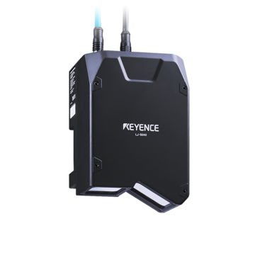
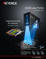
3D Imaging
This method provides a very high level of detail, which gives manufacturers the ability to detect the smallest of defects. Applications for this method are vast, and it applies to fields ranging from semiconductor manufacturing to timber analysis to road surface inspections. The ability to create detailed 3D maps allows manufacturers to not only identify the defects, but also understand their nature.
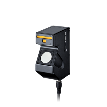
Dark-Field Imaging and Raman Spectroscopy
This technique is particularly useful for detecting scratches, micro-cracks, and other surface imperfections that are difficult to spot under normal lighting. Raman spectroscopy is different, using laser light to analyze molecular vibrations and detect micro-level defects on optical surfaces. By analyzing specific Raman speak, manufacturers can achieve a level of precision that was otherwise unattainable. This method has proven to be invaluable in industries that require flawless surface quality, such as optics manufacturing.
AI-Powered Automated Optical Inspection (AOI)
By integrating machine learning algorithms and computer vision, AI-powered AOI systems can help your organization identify complex defect patterns and adapt to variations in surface textures. Unlike traditional AOI, these systems are constantly improving through training, which allows them to detect scratches, cracks, and other surface defects with remarkable accuracy. AI-powered AOI is very impactful in industries such as electronics and textiles, where high-speed and precise inspections are the essence of quality.
Surface Defect Inspection Techniques for Precision
Ultrasonic and Infrared Thermography
By sending high-frequency sound waves into a material, this method maps the internal structures of a product. This provides real-time insights into hidden defects that could compromise product integrity. It’s a go-to method in aerospace and automotive components where hard-to-detect structural weaknesses can result in operational failures.
Infrared thermography, on the other hand, focuses on surface and near-surface defects by detecting thermal variations. This non-contact, rapid inspection method can identify anomalies in heat flow and conductivity which is ideal in dynamic manufacturing environments. In most industries, thermography is used to detect delaminations, cracks, and inconsistencies in thermal coatings; this helps ensure safety without disrupting production.
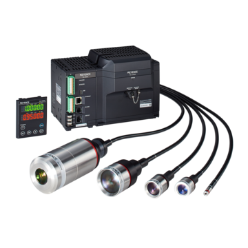
Advanced Calibration and Laser Scanning Techniques
By correcting distortion and ensuring consistent imaging quality, these calibration systems capture incredibly accurate inspections of surfaces. Advanced calibration systems can reconstruct defect images during wafer inspection–meaning the smallest of cracks, defects, and contamination can be analyzed.
Laser scanning technologies further elevate surface inspections by creating high-resolution surface profiles. Laser-based systems quickly identify the smallest of irregularities, including poorly finished edges. The automotive industry, for example, relies on laser profiling to maintain strict dimensional tolerances. Laser scanning is also non-contact and non-destructive, meaning it is an ideal solution for inspecting delicate surfaces.
Benefits of Using a Surface Inspection System
Modern surface inspection systems have redefined accuracy and reliability. They set new standards for quality assurance across all industries. By implementing new technologies like high-resolution cameras and sensors, surface inspections can capture minute details that manual inspections often miss. This capability dramatically reduces false positive as well as false negative inspections, making sure that only genuine defects are flagged. With AI algorithms constantly fine-tuning defect recognition, these systems have been able to adapt to complex patterns with ease while also delivering unparalleled results.
The implementation of automated systems to conduct surface inspections has also reshaped the process. As manufacturers minimize their reliance on manual labor, they can achieve higher throughput without compromising on quality. Real-world applications have shown that these systems can handle huge production volumes while maintaining accuracy, which provides both economic and operational advantages.
Are you ready to take your quality control processes to the next level? Well, get ready to enhance your precision with advanced surface inspection methods from KEYENCE. Our expertly designed solutions empower manufacturers to detect even the smallest of defects to ensure that your product is consistent in quality. Contact our team today to get started or to explore more KEYENCE technologies and how they can transform your inspection needs.