3D Optical Profilometry vs. AFM: When Optical Measurement Wins
Not every surface measurement job calls for the same tool. 3D optical profilometry and atomic force microscopy both map surface topography in fine detail, but they go about it in almost opposite ways. One uses light and never touches the part; the other drags a physical probe across it at the nanometer scale. Picking between them usually comes down to how big the area is, how delicate the sample is, and how much resolution the job actually demands. This guide breaks down how each method works and where optical measurement may be more appropriate.
For a more technical breakdown of the differences in these technologies, please reference: 3D Optical Profilometry vs. AFM - Measurement Physics, Resolution Limits, and Application-Driven Selection
Key Takeaways
- 3D optical profilometry offers fast, non-contact measurement across larger surface areas.
- Atomic force microscopy delivers nanoscale detail but covers smaller areas at a slower rate.
- A 3D optical profilometer suits delicate, soft, reflective, or geometrically complex surfaces well.
- AFM atomic force microscopy may be the better pick when force or surface interaction data is needed.
- Sample type, required resolution, measurement range, and testing speed should all guide the final choice.
3D Optical Profilometry vs. Atomic Force Microscopy
At a basic level, one method uses light while the other uses touch. Optical profilometry bounces light off a surface and calculates height from how the light behaves, so it never makes physical contact with the sample. An atomic force microscope, by contrast, drags an extremely fine probe across the surface and measures the tiny forces between the tip and the material itself. Both approaches produce detailed 3D surface maps, but the underlying physics, and the tradeoffs that come with them, differ quite a bit.
How 3D Optical Profilometry Works
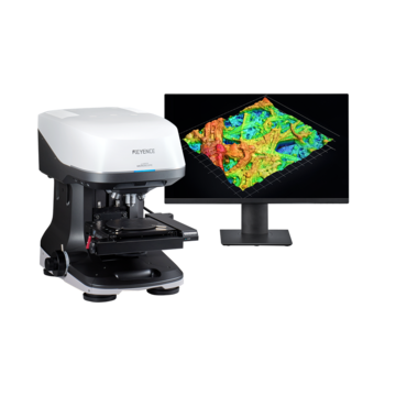
A 3D optical profilometer captures height data by analyzing light reflected from the sample, often using techniques like confocal imaging, interferometry, structured illumination, or focus variation. As the system scans, it records how light intensity or phase changes at each point, then converts that data into a full height map. Because it works with light rather than a mechanical probe, it can cover a wide field of view quickly, and it never risks scratching or deforming a soft or fragile surface in the process.
How Atomic Force Microscopy Works
An AFMworks through direct physical interaction. A cantilever with an ultra-sharp tip, sometimes just a few atoms wide, scans across the sample while a laser tracks how much the cantilever bends. That bending reflects tiny attractive or repulsive forces between the tip and the surface, and the system translates those deflections into a height profile with sub-nanometer precision. A scanning probe microscope like this can resolve individual molecules or atomic steps, details that light-based systems simply can't reach.
Key Differences in Resolution, Speed, and Measurement Area
AFMs win on raw resolution, often reaching down to atomic-scale features. But that precision comes at a cost: scan areas are typically limited to a few hundred microns, and a single scan can take minutes or longer depending on resolution settings. Optical profilometry trades some of that ultimate resolution for speed and reach, covering millimeters or even centimeters of surface in the time an AFM might need to finish a much smaller patch.
When 3D Optical Profilometry Is the Better Choice
Optical measurement tends to win whenever speed, ease-of-use, sample size, or sample fragility becomes the deciding factor. If you need to inspect several parts, or if the material can't tolerate physical contact, optical profilometry usually makes more practical sense than atomic force microscopy.
Measuring Larger Surface Areas Quickly
Because it scans with light rather than a mechanical tip, an optical profilometer can cover broad areas in seconds rather than minutes. This matters a great deal in manufacturing environments where throughput drives the whole inspection process, and waiting several minutes or longer per part simply isn't realistic.
Inspecting Delicate or Soft Materials Without Contact
Soft polymers, thin films, and biological samples can deform or tear under a mechanical probe. Since optical profilometry never touches the surface, it avoids that risk entirely, which makes it a safer choice for materials that need to stay exactly as they were before measurement. Optical 3D measurement systems can also quantify film thickness that a contact-based system is unable to.
Capturing Complex 3D Surface Features
Steep walls, deep trenches, and highly textured surfaces can be difficult for a probe to navigate without losing contact or bending awkwardly. Optical systems, particularly industrial confocal microscopes, often handle these complex geometries more gracefully, building accurate maps even where slopes get steep.
When Atomic Force Microscopy May Be Preferred
AFMs still hold the edge when the application calls for true atomic or molecular resolution, or when researchers need force data, adhesion measurements, or mechanical property information alongside the topography itself. Scanning probe microscopy remains the standard in fields like nanomaterials research and semiconductor development, where that level of detail simply can't be skipped.
How to Choose Between a 3D Optical Profilometer and AFM
Start by asking what resolution the application truly requires, not just what sounds impressive on paper. Many inspection tasks never need atomic-scale detail, and forcing every sample through an AFM just slows things down without adding real value. Consider sample size, fragility, and how many parts need to be measured in a given day, since those factors often matter more than raw resolution alone.
Compare Sample Type, Resolution, Throughput, and Measurement Range
Reflective or transparent materials, along with samples sensitive to contact, generally favor optical measurement. Applications demanding atomic-level detail or force interaction data point toward AFM instead. Throughput needs and the size of the area being measured round out the decision, and matching the tool to the job usually beats defaulting to whichever system happens to be available.
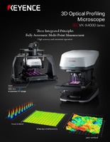
KEYENCE's 3D optical profiling systems combine fast, non-contact 3D measurement with the flexibility many labs need for day-to-day inspection work, and this industrial 3D surface measurement resource covers the topic in more depth.
Frequently Asked Questions
Q What is the difference between 3D optical profilometry and atomic force microscopy?
A
Optical profilometers measure surfaces with light and never touch the sample, while an AFM uses a physical probe to sense surface forces at near-atomic resolution.
Q Why would someone choose AFM over a 3D optical profilometer?
A
When a feature is smaller than the diffraction limit of light, or when true atomic-scale resolution is required, AFM remains the better instrument. It's the right choice for specialized nanoscale research rather than routine measurement.
Q Is 3D optical profilometry as accurate as AFM?
A
For most surface roughness, step-height, and topography measurements, yes. AFM has higher resolution at the atomic scale, particularly for lateral resolution, but 3D optical profilometry provides calibrated, traceable height data that's more than sufficient for the large majority of quality control and materials characterization work.
Q Can 3D optical profilometry measure nanoscale surface features?
A
Yes, many optical systems can resolve nanoscale height differences, though an AFM still leads for true atomic-level detail.
Q Does AFM require special sample preparation?
A
Less than an SEM. AFM doesn't need a conductive coating or vacuum chamber, but it does require a trained operator and a sample that fits within its narrow XYZ measurement range. In addition, a strongly-controlled environment with minimal vibration is required to ensure stable results.