Industrial Laser Marking Systems / Laser Markers
Laser Marking in the Electronics and Semiconductor Industry
-
Tags:
- Laser Marking , Battery , Ceramic
When it comes to semiconductor manufacturing, precision, efficiency, and compliance are key considerations. As the industry evolves, the need for effective identification and compliance solutions has never been greater.
Luckily, electronic marking and laser marking for the semiconductor industry have been up to the challenge. It provides an innovative solution to the way semiconductor components are labeled and tracked throughout their lifecycle. Because of this, manufacturers worldwide have reaped the benefits and improved their operations.
The following will provide an overview of electronic marking technology in the semiconductor industry. We will look at applications of an electric marking machine, like a fiber laser marker or a UV laser marker, how semiconductor laser marking helps with compliance and traceability, and how laser marking technology has become a valuable tool for manufacturers.
Challenges in Laser Marking Electronics and Their Solutions
Electronics manufacturing demands precision and efficiency in all operational tasks. For components like printed circuit boards (PCBs) and microchips to be precisely identified and tracked, laser electronic marking is essential. However, several challenges can arise during the laser marking process.
Reducing thermal damage, for example, is often a challenge. The energy used when laser marking can be damaging, especially to electronic parts like microchips that are heat-sensitive. Circuit distortion from too much heat can result in malfunctions. Semiconductor laser marking systems are needed to solve this problem. The thermal impact is reduced by their short pulse durations and low heat emission design, protecting even the most delicate components.
Marking intricate and odd shapes presents another difficulty. Electronic components often have curved surfaces that make marking more difficult. Achieving uniform markings on these intricate geometries can be difficult. The use of advanced marking machines, such as those from KEYENCE featuring 3D control capabilities, can effectively tackle this issue.
Another major obstacle is material compatibility. Selecting the appropriate laser type for a given material is crucial because different electronic materials respond differently to laser marking.

Factors to Consider When Choosing Laser Markers for the Electronics and Semiconductor Industry
Choosing the right laser marker involves careful consideration. Understanding how each material reacts to laser marking is essential to selecting the best system. First, the material type is a primary consideration. Materials such as plastics and metals like aluminum require different laser technologies.
For marking metals, fiber lasers are often preferred due to their efficiency and ability to create high-contrast markings. Ideal for plastics and metals that are heat sensitive, UV lasers provide clean, crisp markings without causing damage.
Marking speed, particularly in settings with high production volumes, should also be considered. A laser marking system must keep pace with production lines to avoid bottlenecks. Manufacturers can meet production targets without sacrificing quality thanks to KEYENCE's 3-axis laser systems, which offer high marking speeds plus precision.
Since even small mistakes can result in serious malfunctions, accuracy is also essential in the semiconductor industry. The best results can be ensured by marking machines with sophisticated calibration features and fine-tuning options.
Direct Part Marking in the Semiconductor Industry
Semiconductor laser marking is a process that uses a laser marking system to mark semiconductor devices with identifying numbers, barcodes, or logos. The laser marking system directs a beam of high-energy light at the semiconductor device, which heats the surface of the device and causes it to change color. This change in color is used to create the markings that can provide part branding or traceability.
Laser marking semiconductors is an important part of the manufacturing process, as it allows for the easy identification of semiconductor devices. In addition, semiconductor laser marking can be used for other purposes, such as part marking and barcoding.
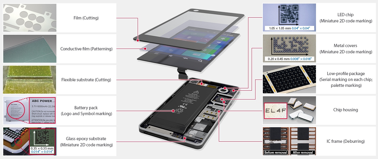
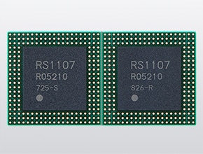
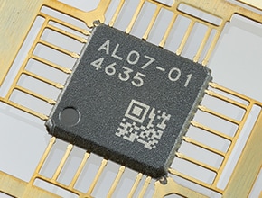
IC packages
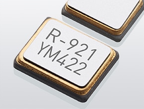
Crystal oscillators
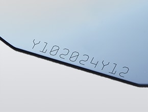
Wafers
Moulded packages
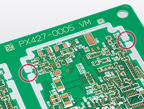
Glass epoxy PCB
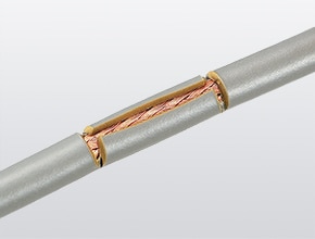
Wire sheath
Epoxy package
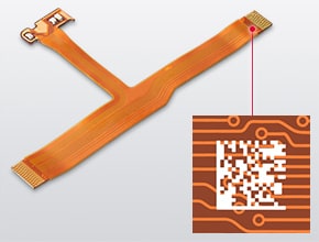
Flexible PCB
Semiconductor manufacturing is the process used to create semiconductor devices, which are electronic components made from semiconductor materials. These materials are typically silicon-based but can also be made from other materials such as germanium, gallium arsenide, or silicon-germanium. The parts are commonly used in computers, hand-held electronic devices (e.g., mobile phones, tablets, and electronic book readers), wearable devices, and consumer electronics.
This manufacturing process starts with wafer fabrication, in which these materials are purified and shaped into thin disks called wafers. These wafers are then subjected to a series of complex processes that add electrical components such as transistors and other circuit elements. Also, many parts require laser marking before they are packaged and shipped to the customer.
Semiconductor manufacturing is a highly complex and precise process, and even small changes in the fabrication process can significantly impact the finished product's performance. That said, using precise and professional equipment is paramount, including the right semiconductor laser marking systems.
These laser marking machines are used to create semiconductor devices such as semiconductor chips, wafers, printed circuit boards (PCBs), integrated circuits (ICs), and other semiconductor devices.

Laser Etching Electronic Components
Considered a subset of laser engraving but not to be confused with its unique process, laser etching entails melting surface material. This creates a process of heating, cooling, and expansion that leaves a detailed mark. The precision and uniformity behind electronic marking are unmatched, but certain characteristics of etching separate the process from the rest.
Here are a few notable characteristics of laser etching:
- A faster process compared to engraving.
- Known for relatively shallow markings.
- Non-contact to help avoid mechanical stressors.
- Capable of high or low contrast markings on small and large electronic components.
- Combines efficiency with consistently readable quality in individual and bulk production.
These few examples cover many angles that have helped propel and innovate within the laser marking semiconductor industry. In the same vein, numerous marking technologies deliver unique benefits and processes for etching tasks. From hybrid to UV laser markers, manufacturers can approach etching semiconductors and electronics in a customized way that fits their production needs.
However, aside from its undeniable versatility, etching isn't always the first choice for some manufacturers. There's more than one reason that several laser marking processes, technologies, and techniques exist. Although there are quite a few similarities, it's helpful to understand the core differences in laser engraving applications and processes.
Laser Engraving Electronic Components
Featuring a slightly different process, laser engraving is a part of electronic marking that vaporizes the material's surface while removing layers. This works to create depth in the mark for designs, logos, barcodes, and more for electronic and semiconductor components.
Another standout point is that the final quality can withstand many other manufacturing processes that are common with electronics. A few examples in this context include:
- E-coating
- Various heat treatments
- Shot blasting
- Electroplating
When it comes to the technologies used for engraving, a variety of electronic marking systems are available to provide different processes and results. For example, many manufacturers utilize fiber laser markers for semiconductor engraving. This is primarily due to its laser wavelength, which is well suited for engraving metal surfaces, as long as they are not heat sensitive.
For those who are new to the topic or simply searching for the most effective process for their needs, it's understandable if there's some trouble in picking a side. Thanks to modern laser marking technologies, you don't always have to choose one over the other. Not only are many laser markers capable of engraving and etching numerous materials, but their efficiency promotes interchangeable manufacturing processes. This gives businesses more flexibility on the production floor.
The full scope of laser engraving applications in the realm of electronics and semiconductors goes a long way. You can say the same for etching processes. Both marking techniques are highly flexible to a variety of marking needs when it comes to semiconductors and a never-ending list of electronics.
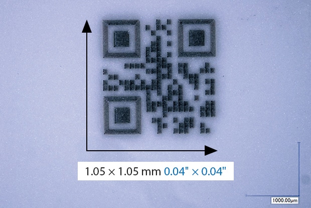
Micro and 2D Code marking on IC Chips
Until recently, IC chips were only marked with lot codes. However, a growing need for encoded data has prompted many manufacturers to start using 2D codes. These 2D codes provide unique identification and offer a wealth of encoded data, including batch information, production details, and other relevant information. This transition reflects the industry's commitment to using advanced marking technologies to meet changing requirements and ensure product integrity.
Here are a few common methods for micro and 2D code marking that a semiconductor laser marking machine might use:
Micromarking
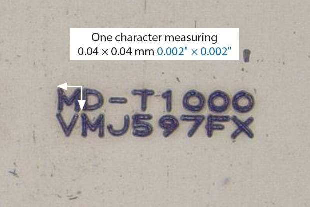
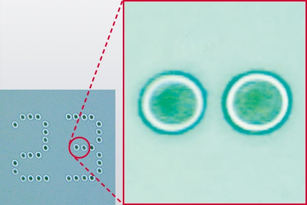
Laser markers have a very small beam spot, making them perfect for applications with a limited marking area. Micromarking - which is typically impossible for most systems - can be accomplished with the right laser. Various marking styles can also be selected, from shallow marking to deep engraving. Because of the minuscule sizes of semiconductor components, it enables tasks that were once deemed unattainable by conventional marking systems.
Marking silicon wafer
Silicon wafers are delicate components that require precise marking. It's vital to keep surface damage to a minimum when marking a finished wafer. If not, dust and debris can form. Damage during the marking process can lead to contamination risks, compromising the quality and performance of the finished wafers. That's why UV and green lasers are the optimal wavelengths for these applications. They provide the controlled marking that is needed without causing surface damage.
Marking LED ceramic package
The compact nature of LED ceramic packages poses unique challenges for traditional marking methods. Due to space limitations, ceramic packages often use 2D codes to contain all the necessary traceability information. By incorporating 2D codes on LED ceramic packages, manufacturers can easily embed batch information, production details, and other critical data. This streamlines the tracking and identification process, enhances supply chain visibility and quality assurance efforts, and ensures compliance with industry standards.
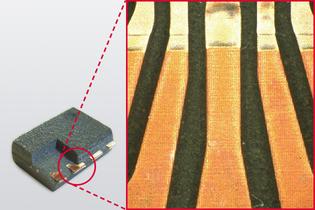
Plating and Coating IC Chip Removal
KEYENCE’s 3-Axis laser markers can mark the top surface of IC chips and remove plating or coatings within the same process. Since the laser accurately scans only along the edges of the IC, flash burrs over the leads can be removed without causing damage to the inside of the package.
Removal of gold plating on terminals
To prevent solder wicking, lasers are used to remove the gold plating from connector terminals.
In the past, masks were used to avoid unnecessary plating. Today, connectors are smaller and thinner, and the pitches between the terminals are narrower. Consequently, it has become common practice to apply plating and then remove it with a laser for micron accuracy.
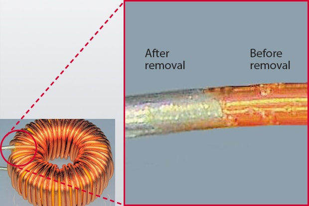
Removal of thin-film coil coating
Previously, removers or edged tools were generally used to remove thin-film coating from coils. Now, laser markers have become useful because they require no consumables and ensure stable results.
Resin coating removal
Chemicals are often used to remove resins on defective molds so that the molds can be analyzed. However, chemicals can damage the internal circuit and require multiple man-hours of work. Using a laser marker to remove resin saves running costs and time.
Benefits of Laser Marking Semiconductor Parts
In the semiconductor industry, semiconductor laser marking is used extensively for part marking. This is because semiconductor laser marking machines offer many advantages over other types of machines.
For example, semiconductor laser marking machines can mark very small parts with a high degree of accuracy. This is a critical requirement of an electronic marking system since the tiny semiconductor components demand microscopic detail.
In addition, semiconductor laser marking machines are very fast, so they can mark large quantities of parts in a short period of time. This allows manufacturers to produce a large quantity of parts within short time frames, which is often needed to meet demand and production schedules.
The process is also highly versatile, allowing for a wide range of semiconductor part designs and markings. This includes silicon wafers, crystal oscillators, lead frames, and IC packages.
Additionally, semiconductor laser marking is an environmentally friendly alternative to other part marking processes, such as labels or screen printing, because it does not use any consumables. As a result, semiconductor laser marking machines are an essential part of the semiconductor industry.
Specific Applications of Laser Etching and Engraving Within the Semiconductor Sector
While the topic of the semiconductor industry is quite broad, etching and engraving serve more of a purpose than just identification alone. From individual components to the packaging they’re shipped in, both semiconductor etching and engraving are being actively used as we speak. For a more in-depth look at specific applications, the bullet points below offer some active use cases of the electronic marking processes.
- Numerous EV laser marking applications
- Tamper evidence, as well as anti-counterfeiting for semiconductors and individual components
- Reliable identification and part traceability
- Making changes to surface materials for better adhesion, reflectivity, and more
- Branding and product customization
- Creating marks that can withstand other harsh machining processes without losing clarity
- Marking PCB boards and cutting electrical insulation foils that segment components
- Precision markings for surface mount devices (SMDs)
This list would just continue from there, supported by more points that highlight the capacity and flexibility of the laser marking semiconductor industry. It’s important to mention that getting the most out of these laser marking processes requires working with reliable technology and topical experts.
This is where our support at KEYENCE comes into play. We can help bridge your understanding and application of laser marking technologies, as well as the many manufacturing processes they’re capable of.
Laser Marking Technologies for the Electronics and Semiconductor Industry
There are different types of semiconductor laser marking and laser electronic marking technologies available, and each is appropriate for a particular use in the semiconductor and electronics industries. Plastics and thin films used in semiconductor packaging are among the delicate materials that UV lasers are especially good at marking. With little heat input, these lasers lower the possibility of damaging delicate parts like microchip serial numbers and barcodes.
However, metals like stainless steel and aluminum, which are frequently found in circuit boards and electronic housings, are perfect for marking with fiber lasers. Fiber lasers create clean, deep engravings that are resistant to wear and corrosion, ensuring longevity and traceability.
For marking delicate materials like silicon wafers and particular polymers, UV lasers are becoming more popular. They are great for applications that call for incredibly fine markings because of their high precision and decreased vulnerability to heat damage.
KEYENCE - The Right Laser Marking Partner
A range of laser marking solutions designed to satisfy the particular requirements of the semiconductor and electronics industries are offered by KEYENCE. We serve as an extension of your team to help you improve and automate your factory. Additionally, our knowledgeable team and trained sales force can help solve challenging and technical problems related to semiconductor part marking.
Contact us to see how our robust systems help with laser marking electronic components and semiconductor parts.

Application Video
FAQs about Laser Marking in the Semiconductor Industry
What types of lasers are used in wafer manufacturing?
Two of the most common types of lasers used in wafer manufacturing are near-infrared and UV lasers. Historically, near-infrared lasers have been the industry standard, but new developments in UV systems have shifted the needle in their favor.
Why do semiconductor wafers need to be laser-marked?
Traceability is the driving factor behind laser marking in this industry. Semiconductors go through many steps prior to distribution, so it is important to have 100% traceability to ensure each procedure has been met and faulty products are separated before reaching the customer.
What are the challenges of laser marking in the semiconductor industry?
As advancements in this industry continue, components also shrink in size. This level of intricacy highlights the need for premium beam control and limited heat-affected zones. In addition to increasing demand for precision, the general application scope tends towards a more technical need. KEYENCE stands alone in providing local product specialists to work with your team to see how lasers could benefit your process.
How are lasers used in semiconductor manufacturing?
Historically, lasers have been used to mark content for traceability or branding purposes. Recent advancements have opened the door to a new realm of applications when it comes to laser processing. The same lasers used for traceability have the capability to precisely alter surface properties or remove material making lasers a versatile tool for semiconductor manufacturers.
What types of materials can be laser-marked in semiconductor manufacturing?
Laser marking can be performed on a wide range of materials, including silicon, silicon carbide, gallium arsenide, and various types of metals and ceramics.
How does laser marking contribute to quality control in semiconductor manufacturing?
Laser marking provides a permanent and legible mark on semiconductor wafers and components. This ensures accurate identification and traceability throughout the manufacturing process. As a result, it helps to prevent errors, reduce waste, and maintain quality standards.
What factors should be considered when selecting a laser marking system for semiconductor manufacturing?
When choosing an electronic marking system, you should consider laser wavelength, power output, marking speed, beam quality, and the ability to achieve precise marking. Additionally, compatibility with existing manufacturing processes and integration capabilities are important considerations.
Can laser marking be used for other applications besides traceability in semiconductor manufacturing?
Yes, semiconductor laser marking has a wide range of applications beyond traceability, including surface texturing, micro-machining, microstructuring, and surface modification. These capabilities make laser marking a versatile tool for semiconductor manufacturers looking to enhance product performance and functionality.
Related Downloads
![Laser Marker Installation Examples [Electronic Device Industry]](/img/asset/AS_117224_L.jpg)