Industrial Laser Marking Systems / Laser Markers
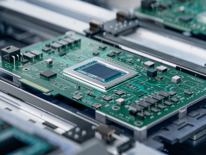
Laser Marking PCBs
-
Tags:
- Laser Marking , Laser Cutting , Laser Drilling
Key Takeaways
- UV laser marking gives permanent, high-contrast IDs on FR-4, polyimide, and ceramics with minimal HAZ.
- Use low pulse energy, high repetition, and multi-pass recipes to build contrast while limiting thermal load.
- Integrate vision, ISO/IEC 15415 or 29158 grading, and IPC-1782 data flow to automate verification and MES logging.
- 3-axis beam control and autofocus preserve spot size across warp, mixed heights, and near-components.
- For depaneling/drilling, prefer multi-pass contour or trepan toolpaths and strong fume extraction to reduce char.
Printed circuit boards sit at the heart of every electronic product, and their identification requirements have grown with traceability, quality, and regulatory demands. Laser marking meets these needs with precise, permanent, and readable IDs that survive reflow, washing, and handling. On common materials—FR-4 solder mask, polyimide flex, and ceramics—UV lasers create high-contrast marks with minimal heat-affected zone, making them well suited for serial numbers, lot codes, and compact 2D symbols.
Advantages of Laser Marking in the PCB Industry
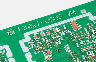
Laser marks are permanent, high-contrast, and repeatable without consumables such as ink or labels. UV wavelengths are effective on solder mask, polyimide flex, and ceramics with minimal heat-affected zone. Fine spot sizes support compact Data Matrix or QR codes in small keep-out areas. Integrated code verification streamlines compliance with U.S.-relevant standards like IPC-1782 for traceability and ISO/IEC 15415 or 29158 for code grading.
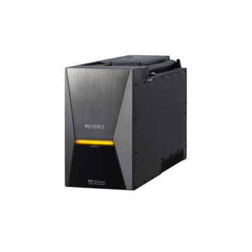
In aerospace and defense, robust PCB marking also supports device-level UID practices under MIL-STD-130. Features such as 3-Axis beam control and autofocus maintain focus across warped panels and mixed component heights, while low-maintenance designs and safety packages suit continuous SMT/PCBA operation. The MD-U2 UV laser exemplifies these advantages on FR-4, polyimide, and ceramic substrates.
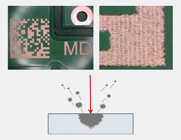
Magnified images obtained by VHX microscope
By nature, IR lasers use heat to create markings. The high peak power created by the hybrid oscillation structure mitigates the impact of this vs standard fiber lasers.
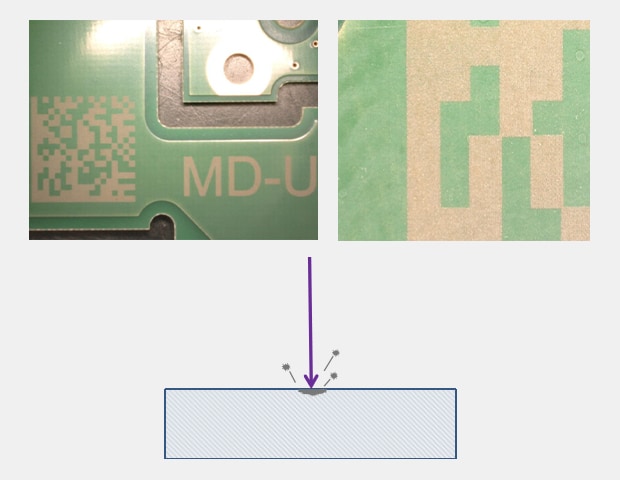
Magnified images obtained by VHX microscope
Due to its shortened 355 nm wavelength, the absorption rate of UV laser light skyrockets. This allows the MD-U to perform "cold marking" completely negating any thermal impact to the FR-4 Coating and keeping the underlying copper untouched.
PCB Laser Etching: Everything You Need to Know
On PCBs, “etching” usually means removing a thin layer of solder mask or coating to create contrast. On FR-4 with green solder mask, UV energy cleanly ablates pigment and binder for crisp codes and text. On polyimide flex, UV reduces charring and preserves mechanical strength compared with longer wavelengths. On alumina or aluminum nitride ceramics, UV produces dark, legible marks with tight edge definition. Conformal coatings can be selectively marked or removed; integrated vision helps align to post-coat features. Practical starting points include low pulse energy, high repetition rate, and multiple fast passes to build contrast with minimal thermal load. 3-Axis beam control preserves spot size across bow, warp, or step heights, and verification after reflow, wash, and coat confirms long-term readability.
Conventional
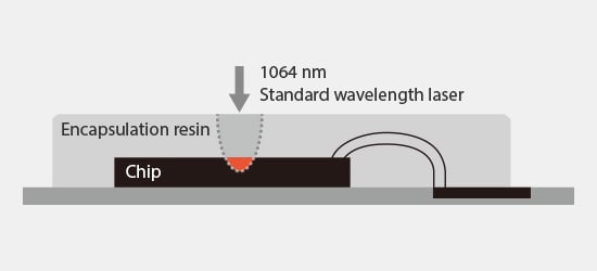
Internal damage caused by laser light transmission
As electronic components such as mobile terminals become smaller every year, the thickness of the encapsulation resin that covers internal devices has also become thinner. As a result, there is a concern that laser energy transmitted through the encapsulation resin will cause internal damage when using a standard wavelength laser.
MD-U
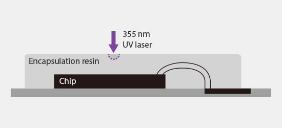
Transmission is suppressed due to the high absorption rate
Because UV lasers have a high absorption rate, the laser light is absorbed by the surface of the encapsulation resin, which can reduce internal damage.
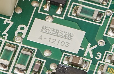
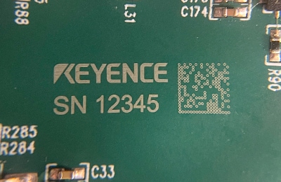
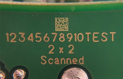
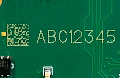
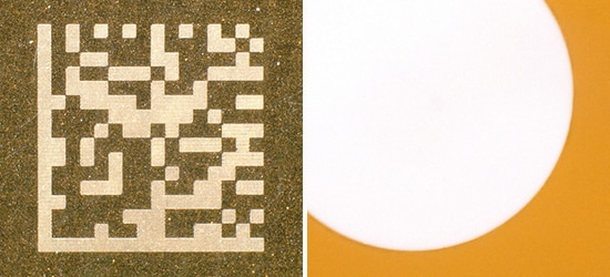
Laser Engraving Serial Numbers on PCBs
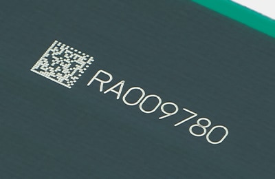
Serial numbers, date codes, and 2D Data Matrix are common on both boards and assemblies. Data Matrix is favored for high data density and robust decoding in small cells. Typical locations include solder mask windows, underside areas, or stiffeners on flex; fiducials nearby simplify alignment. Integrated vision can locate the board, apply offsets, and immediately read and grade the result to ISO/IEC 15415 or 29158, with grade images exported to MES or quality systems to support IPC-1782. UV wavelength reduces delamination risk and helps maintain solder mask integrity. Shallow engraving recipes and 3D height correction help place marks near components without compromising nearby pads or traces.
Implementing Laser Marking of Printed Circuit Boards
Begin by defining the data strategy: serials, lot/batch, PCB revision, and MES transaction IDs, along with when to mark (bare board, post-SMT, post-ICT, or post-coat). Align content and verification with IPC-1782 and adopt ISO/IEC 15415 or 29158 grading practices. Select wavelength by material; UV (e.g., MD-U2) is versatile for solder mask, polyimide, and ceramics, while fiber and CO2 are more typical for metals and certain organics. Choose working area and establish low-energy, multi-pass recipes. Confirm durability after thermal cycles, washing, and coating and connect the station to MES to receive serials and return pass/fail grades with stored images for audit trails.
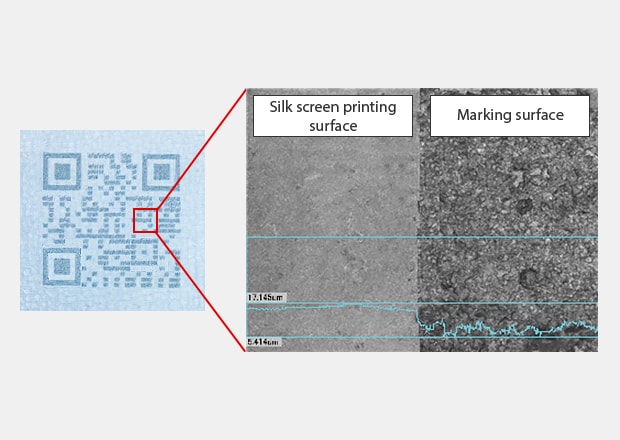
On a silk screen layer, it is possible to carry out the marking without the silk peeling. Due to variations in the thickness of the print itself, delicate stable marking needs to be performed without breaking the layer.
With the increased capabilities of a YVO4 laser, it is possible to control power and energy deliverance at a higher level for delicate target surfaces. To ensure the best results, testing both laser types is recommended.
Laser Marking in PCB Assembly (PCBA)
Marking is commonly placed in-line before pick-and-place, between reflow stages, or after final assembly depending on accessibility and contrast. In-line stations reduce extra handling; off-line cells suit NPI and rework. ESD-safe enclosures and proper fume extraction protect sensitive electronics; UV marking generates minimal debris compared with mechanical processes. When marking near shields or connectors, 3D height correction maintains focus without refixturing. Validate code readability after wash and conformal coat; if coating fills cells, mark pre-coat or adjust parameters to maintain contrast.
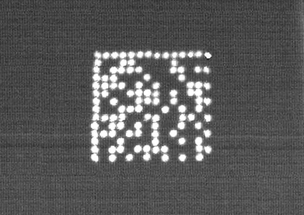
A barcode reader was used to confirm the quality and stability of marked codes and achieved 100% reading results. Since the materials used in PCBs can be very heat-sensitive, too much heat can distort or ruin a mark. Precise control of the heat and energy during marking helps to ensure a highly visible, crisp mark.
Laser Cutting PCBs: Everything You Should Know
Depaneling uses higher power to cut through the board rather than creating surface contrast. UV and CO2 are common for cutting organics, with parameters tuned to limit char and glass-fiber protrusion on FR-4 and to keep edges clean on flex. A multi-pass contour at lower power, instead of a single high-power pass, typically yields the best results and minimizes heat-affected zones. Even with cutting at minimal heat, effective fume extraction is still required at the head to capture particulates and maximize cutting efficiency.
FPC (Polyimide): Marking/Cutting Process With Reduced Heat Damage
Conventional
MD-U
How Does Laser Drilling Work in PCBs?
Lasers can precisely open features in many PCB materials: blind/buried microvias, via-in-pad, coverlay and solder-mask openings, tiny vent holes or slots in rigid-flex, and cutouts in flex tails. UV lasers (355 nm) are popular for clean, small features in dielectrics; IR (1064 nm) or green (532 nm) may be added to remove thin copper “caps” or to help expose the capture pad.
How the process works:
- The laser is focused on the board surface and fires short pulses. Each pulse removes a thin layer of dielectric (controlled ablation).
- Vision or endpoint detection watches for the reflective copper underneath. The system stops or switches to a low-energy “clean” pass to expose the pad without damaging it.
- For round, low-taper holes, the toolpath may trepan (small circular path) rather than drill in place.