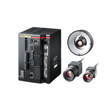
Machine Vision
How AI Vision Systems Improve Semiconductor Manufacturing
Key Takeaways
- AI vision detects wafer defects by learning normal variation, reducing false alarms vs fixed rules.
- Subpixel measurement and 3D imaging enable stable overlay verification and package bump/coplanarity checks.
- In-line AI adapts with production data, shortening setup time and lowering manual review and throughput interruptions.
- Balancing resolution and speed: AI prioritizes relevant image features to maintain throughput while finding subtle defects.
- Inspection data feeds process control and trend analysis, enabling earlier interventions to improve yield.
As each semiconductor wafer moves through hundreds of tightly controlled steps, there is little room for error. A small defect or shift in position can affect the yield of the run, delay performance, or reduce device performance. Inspection systems are installed to help shoulder that pressure. These systems help detect issues early and help wafers remain consistent across batches. Due to the fragile nature of a semiconductor, the balance can be harder to maintain with additional approaches.
AI vision systems that are used in semiconductor manufacturing environments change how these inspections are handled. Instead of relying on a fixed set of rules, these systems can evaluate patterns across image data and adjust to variations along the line.
Challenges in Semiconductor Inspection
Inspection is not a single or solitary step. Inspection stations should appear throughout fabrication, packaging, and final testing, and each stage introduces different risks that can compound (if not discovered) as the process continues.
At advanced stages, features of semiconductor wafers are measured in nanometers. Layer-to-layer alignment has to remain stable across temperature changes and long production cycles, as even small placement errors can affect circuit behavior.
Surface inspection brings its own complications. Wafer patterns repeat across large areas, which makes it difficult to separate real defects from normal variations where texture, lighting differences, and minor cosmetic changes can all trigger false alarms.
There is also a constant tradeoff between speed and detail. Higher resolution reveals smaller defects, but it can also limit throughput if the system cannot process images quickly enough. At the same time, relying on faster, lower-resolution checks increases the risk of missed defects.
Some defects may appear early in the process and are not captured through electrical validation. By the time they surface, any additional work has already been done on their part.
These conditions make inspection less about isolated checks and more about maintaining consistency across a changing process. AI machine vision semiconductor inspection systems are built around that need.
How AI Vision Systems Detect Wafer Defects
AI vision systems for semiconductor manufacturing lines use a combination of imaging, measurements, and pattern recognition; after the system captures data, it evaluates it against learned patterns and flags variation that falls outside of the expected behavior.
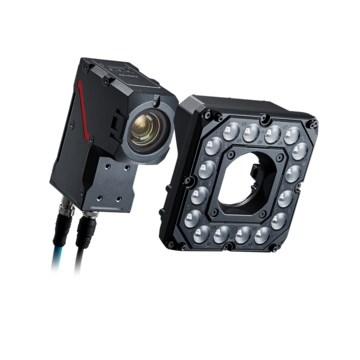
Image Capture and Lighting Control
Inspection begins with controlled imagining. Cameras work with lighting setups that highlight specific surface features. Bright-field and dark-field illumination, for example, reveal different types of defects depending on how the light interacts with the wafer being inspected.
Learning From Real Production Data
AI models are trained using examples of real-life production data from both acceptable and defective parts. Over time, the system builds a reference for normal variation. Instead of applying strict thresholds, it compares new images to the reference.
AI vision systems enhance semiconductor defect detection by identifying subtle, non-patterned defects and filtering out harmless variations that would otherwise cause alerts. These systems often combine AI classification for visual interpretation with rule-based checks for deterministic measurements (like position or distance).
Measurement and Alignment
Vision systems measure features at subpixel resolutions, which supports alignment tasks such as wafer notch detection and overlay verification. The positioning of a part is not static throughout production; systems need to account for rotation and minor deformation when locating features. This allows alignment checks to remain stable across different batches and conditions.
Extending Inspection With 3D Data
3D imaging is used to evaluate height, structure, and surface variation beyond what 2D inspection can capture. This helps identify voids and irregularities that would otherwise go undetected. In packaging, 3D inspection measures bump height, spacing, and coplanarity, factors that directly impact electrical performance and reliability. At KEYENCE, systems like the XT handle this using rules-based tools, delivering consistent, repeatable measurements without relying on AI.
Adapting Over Time
Production runs are also not consistent. Lighting conditions shift throughout the day, and product materials vary. AI models can be updated with new image data, which allows the system to adjust to a new design or an error without a full reset. This keeps wafer inspection automation aligned with real production conditions instead of having to rely on static configurations.
Benefits of AI Vision Systems in Chip Manufacturing
The impact of AI vision systems for semiconductor manufacturing environments shows up in how inspection data is handled and how quickly decisions can be made.
Detection systems have to be more selective. By focusing on pattern variation rather than on fixed limits, the systems reduce unnecessary alerts while still working to identify defects that matter.
AI inspection systems also have to stay in step with the production run. AI visual inspection manufacturing systems operate in-line, having been integrated with existing processes and equipment, so parts are evaluated as they move through the process rather than being pulled out for separate checks.
Manual reviews also decrease as the number of false defects drops. Operators spend less time verifying acceptable parts, which helps maintain a steady production flow.
Earlier detection changes how defects affect yield as well. When issues are found before additional processing steps, there are fewer materials and time lost, which supports a more stable output across batches.
Inspection data also becomes more useful in AI visual inspection in manufacturing. Trends in defect patterns can point to shifts in equipment behavior or process conditions; however, instead of reacting after a failure has occurred, teams can respond while production is still running.
Real-World Applications of AI Vision in Semiconductor Production
AI machine vision semiconductor inspection systems are applied across the full production flow, with each stage focusing on different inspection targets.
In wafer fabrication, systems inspect surfaces for contamination and early-stage damage. These checks happen before additional layers are added, which limits the impact of defects on later steps.
Alignment is verified at several stages, especially before additional layers are added. Wafer notches and fiducials provide reference points for orientation and positioning, helping maintain overlay accuracy.
During packaging, inspection has to focus on the physical structure. Systems measure structural features such as bump height and spacing, and they evaluate bonding quality at a microscopic level.
Wire bonding inspections are another common use case. Vision systems analyze bond position and integrity, which helps identify gaps or misalignments that could affect performance.
Traceability runs alongside these checks. AI-driven systems read codes and markings on wafers and components, even when those markings are partially degraded. This allows parts to be tracked across the entire production cycle.
Each of these applications shows how AI visual inspection in manufacturing integrates direction into a production line without needing to interrupt throughput.
The Future of AI-Powered Semiconductor Inspection
AI vision systems in semiconductor manufacturing environments are becoming more connected to the rest of the production environment. Inspection data is starting to feed into process control systems, and instead of only identifying defects, vision systems contribute to adjusting parameters during production.
Learning models are also becoming more efficient. Systems require fewer examples to adapt to new products or conditions, which helps shorten setup time.
Over time, inspection will play a larger role in maintaining process stability. Systems will continue to move toward operation with fewer manual (human) adjustments, while still providing detailed feedback to production conditions.
Have questions about AI vision systems? Our team is here to help. Contact us today!