Known as a pioneer in fine ceramics, KYOCERA Corporation supplies advanced electronic components worldwide, including ceramic packages for high-performance semiconductors. At the Shiga Higashiomi Plant, the KEYENCE 3D Laser Snapshot Sensor LJ-S8000 Series was introduced to automate the visual inspection of those ceramic packages. The 100% visual inspection once handled by around ten operators at binocular microscopes has been systematized, speeding up inspection by roughly 1.5 times and eliminating variation in accuracy between operators.
Highlights of this case
- KYOCERA Corporation's Shiga Higashiomi Plant introduced the KEYENCE 3D Laser Snapshot Sensor LJ-S8000 Series for the visual inspection of ceramic packages that cover semiconductor chips.
- Before the installation, every package produced was inspected by around ten operators taking turns at binocular microscopes, leaving accuracy dependent on individual skill and speed vulnerable to fatigue.
- The LJ-S8000 Series measures shape, height, thickness and width automatically and instantly in 3D, and judges parts outside the standard values with a pre-set program. Micron-order accuracy and calibration certificates were also valued.
- Since introduction, overall inspection efficiency has risen by about 1.5 times and variation between operators has disappeared. A conveyed pallet is inspected in roughly two seconds.
- Time that operators previously spent tied to the inspection station is now spent on printing work, improving productivity and stabilizing the supply of parts to downstream processes.
ChallengeWhy 100% visual inspection was reaching its limit
The Shiga Higashiomi Plant produces the ceramic packages that cover semiconductor chips. IC packages can also be made of resin or metal, but as chip circuits have grown finer and the spread of AI has driven a huge increase in computation, demand for heat-resistant ceramic packages has expanded rapidly. Having manufactured fine ceramic products since its founding, KYOCERA can apply its technology and know-how directly to ceramic packages, which are now one of its main products.
A ceramic package is not merely an exterior part: it is an electronics component with fine electrical wiring on its surface. Because ceramic itself does not conduct electricity, a metallization process applies metal to the surface to form the wiring pattern. Visual inspection checks whether that pattern has been formed as designed, whether patterns have bridged or become faint, and whether foreign matter has adhered. Before the LJ-S8000 Series, all of that was done by around ten operators taking turns at binocular microscopes.
"Because the work relied on the operators' eyesight, variation in inspection accuracy according to individual skill was a major issue. Even veteran operators could not avoid a drop in inspection speed as fatigue built up over several hours."
SelectionWhat made the LJ-S8000 Series the right choice
The first deciding factor was accurate imaging and measurement of the very fine widths of the electrical circuits under inspection. Those surface circuits are formed by applying a pattern of conductive ink and then sintering it. In the process, thickness or height can fall outside the standard values, a line of ink can develop a gap, or foreign matter can adhere. Any of these can interfere with correct operation of the IC chip, so verifying that the circuit has been properly formed — across a wide variety of product types — was essential.
The LJ-S8000 Series measures shape, height, thickness and width automatically and instantly in 3D, and uses a pre-set program to identify parts that deviate from the standard values. Fine circuit patterns had been difficult to inspect, but the ability to work to micron-order accuracy and to issue a calibration certificate was also cited as attractive.
"The LJ-S8000 measures shape, height, thickness and width automatically and instantly in 3D, and judges parts outside the standard values with a pre-set program. We were convinced it would dramatically improve the efficiency of our inspection."
ResultsWhat automation changed on the inspection line
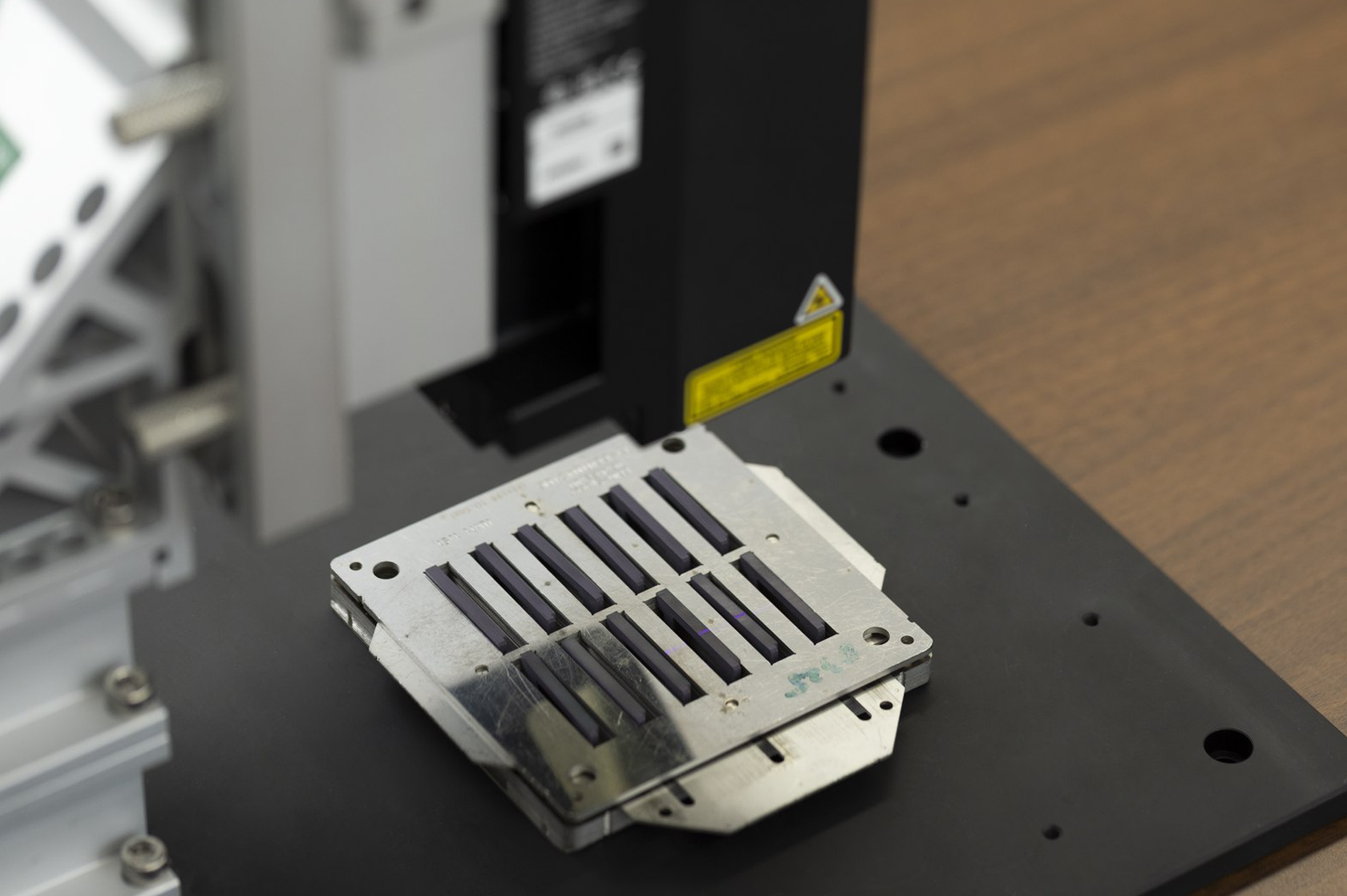
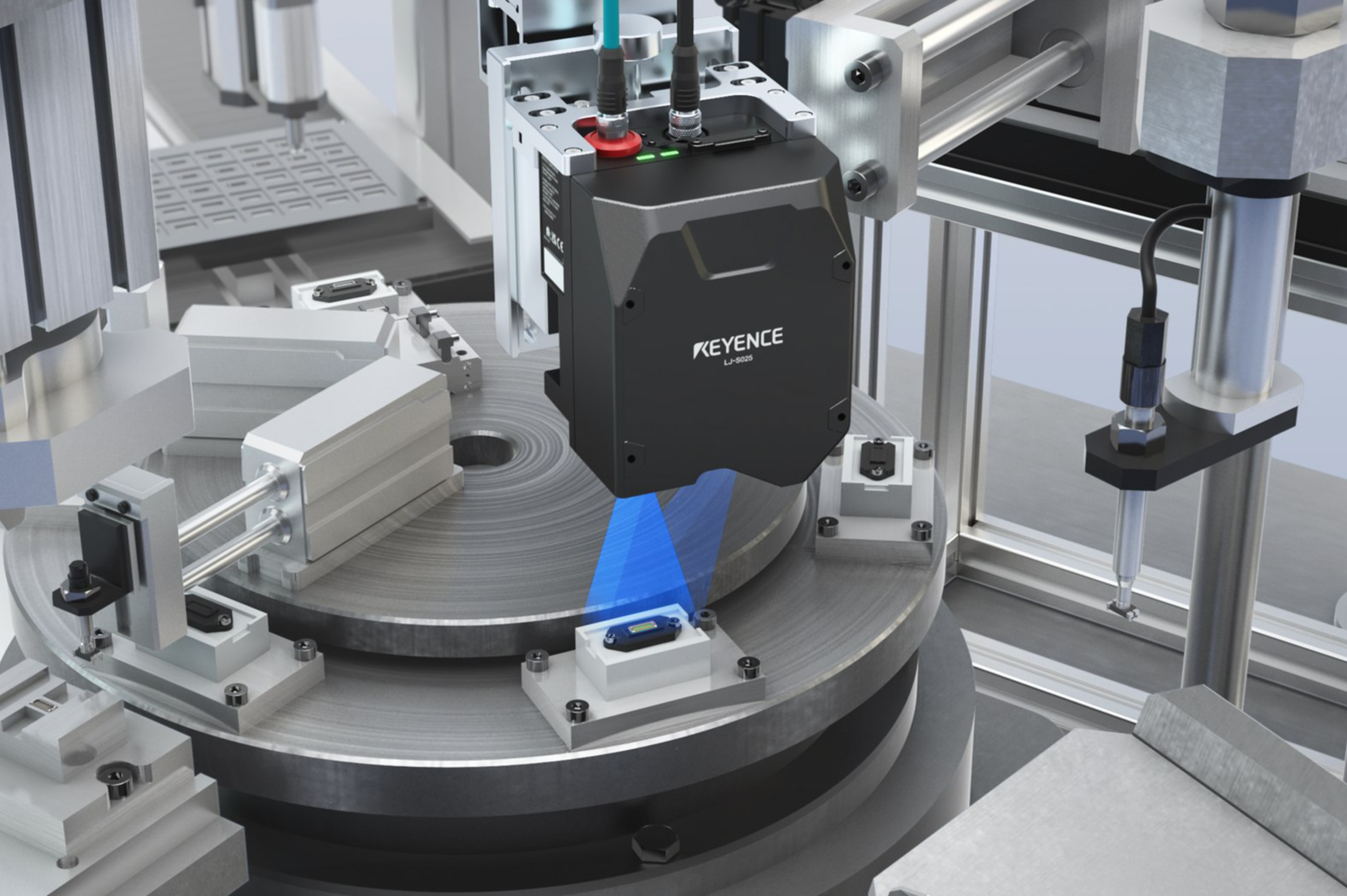
Systematizing an inspection that had relied on human senses sped up overall inspection by about 1.5 times and removed variation in accuracy between operators. Previously, an operator placed a pallet of 16 parts on the inspection table by hand and looked through a microscope — a slow and labor-intensive routine. Today, pallets carrying the parts are conveyed across an inspection table fitted with the LJ-S8000, and one pallet is inspected automatically in about two seconds. A mechanism was also built in to raise an alert with sound and light in the event of a defective part.
"An operator used to have to stay with the inspection the whole time, but because the equipment inspects automatically, that time can now go straight into printing work — which has improved our productivity."
Being able to supply downstream processes with consistently stable parts is another benefit the plant highlights. The project began with an inquiry from KYOCERA to KEYENCE, and from that first contact the sales representative visited the plant frequently, built an accurate understanding of the issues on the floor, and supported the work in detail through to an inspection setup that maximized efficiency — including repeated three-way discussions with the equipment manufacturer, both in person and online.
"Having them become part of the team pursuing the mission of inspection automation was hugely appreciated. At the trial stage it was immediately clear that the inspection specifications we wanted could be fully achieved, so we had no hesitation about going ahead."
OutlookMeeting the demands of the 3D packaging era
Having seen the results of this installation, the plant is considering adding more units. The next equipment under consideration would change the orientation of each incoming part in turn and inspect the circuit patterns on three side faces automatically, using three LJ-S8000 units.
Behind that lies a shift in the semiconductor market itself. The chips used in high-performance semiconductors have miniaturized their circuits almost to the limit, making further performance gains from a single chip difficult. To break through that ceiling, technology that combines multiple chips at extremely short distances in a 3D package has become important — and delivering it demands even higher precision from the circuits on the ceramic package.
"By developing and producing products that answer those global needs, we aim to contribute further to society."
Frequently asked questions (FAQ)
Q What does KYOCERA's Shiga Higashiomi Plant inspect with the LJ-S8000 Series?
A
The visual inspection of the ceramic packages that cover semiconductor chips. Because ceramic itself does not conduct electricity, a metallization process applies metal to the surface to form the wiring pattern. The LJ-S8000 checks whether that pattern is formed as designed, whether patterns have bridged or become faint, and whether any foreign matter has adhered.
Q How was ceramic package inspection carried out before the LJ-S8000 Series?
A
Every ceramic package produced was inspected visually, with around ten operators taking turns at binocular microscopes. Because the work relied on the operators' eyesight, accuracy varied with individual skill — and even veteran operators could not avoid a drop in inspection speed as fatigue built up over several hours.
Q What was the deciding factor in adopting the LJ-S8000 Series?
A
The first deciding factor was accurate imaging and measurement of the very fine widths of the electrical circuits being inspected. The LJ-S8000 measures shape, height, thickness and width automatically and instantly in 3D, and judges parts outside the standard values using a pre-set program. Micron-order inspection accuracy and the ability to issue a calibration certificate were also cited as attractive.
Q What results has the LJ-S8000 Series delivered?
A
Systematizing an inspection that had depended on human senses sped up overall inspection by about 1.5 times and removed the variation in accuracy between operators. Today, pallets carrying the parts are conveyed across an inspection table fitted with the LJ-S8000, and one pallet is inspected automatically in about two seconds.
Q What kind of support did KEYENCE provide during the introduction of the LJ-S8000 Series?
A
From the very first inquiry, the sales representative visited the plant frequently, developed an accurate understanding of the issues on the floor, and supported the project in detail through to an inspection setup that maximized efficiency. The representative also joined repeated three-way discussions with the equipment manufacturer, both in person and online, as part of the team pursuing inspection automation.
Q How does the plant plan to use the LJ-S8000 Series going forward?
A
Having seen the results of this installation, the plant is considering adding more units. The next line of equipment under consideration would change the orientation of each incoming part in turn and inspect the circuit patterns on three side faces automatically using three LJ-S8000 units.