Industrial Laser Marking Systems / Laser Markers
Laser Marking Wafers In The Semiconductor Industry
-
Tags:
- Semiconductor , Laser Labeling , Laser Etching
Key Takeaways
- UV laser "cold" marking minimizes heat-affected zone (HAZ) and reduces surface damage on wafers.
- 3-axis autofocus maintains focus across wafer flatness variations for uniform, high-resolution marks.
- Low-fluence, high-rep-rate, fast-scan parameters produce high-contrast marks with minimal debris.
- Inline vision inspection and MES logging verify readability and enable automatic re-marking or flagging.
- Backside/scribe-line marking and fume extraction preserve FEOL/BEOL integrity and cleanroom compatibility.
Semiconductor wafers move through hundreds of process steps, from crystal growth to singulation. At critical points along that journey, manufacturers apply permanent identification so every wafer, lot, and die can be traced. Laser marking is the preferred method because it is non-contact, precise, cleanroom-friendly, and capable of producing high-contrast, durable characters and codes at high speed—without adding consumables.
The following guide explains how wafer laser marking fits into modern semiconductor production. It also highlights practical choices that matter to engineers and operations leaders—like surface damage risk, debris control, automation, and verification—along with how a UV laser such as KEYENCE’s MD-U2 addresses those priorities.
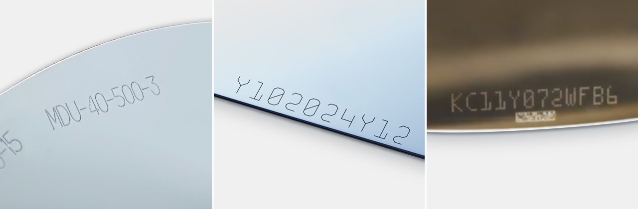
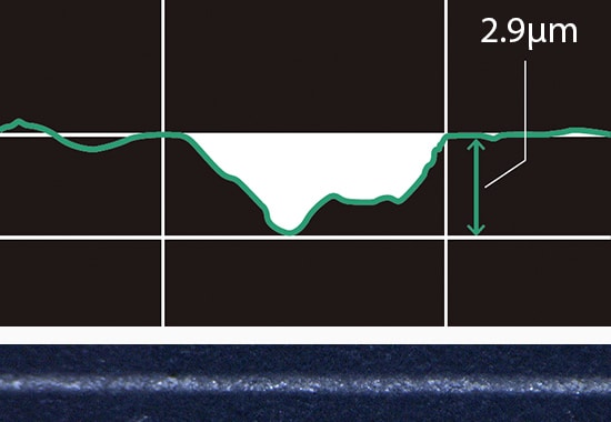
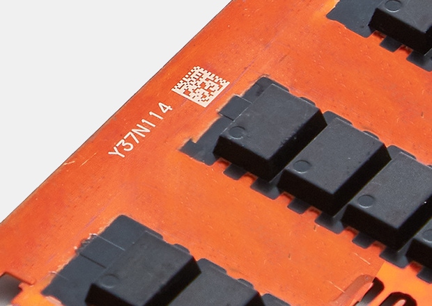
Wafer marking examples

Laser Marking Techniques for Si and Ga Wafers
Silicon (Si) and compound semiconductors such as gallium arsenide (GaAs) and gallium nitride (GaN) can be marked via several mechanisms, each optimized for low slag and clean edges:
- Surface discoloration/photochemical change: UV interaction can modify surface chemistry for contrast with minimal ablation.
- Micro-ablation: Very shallow, precise material removal tuned below crack-initiation thresholds.
- Passivation-friendly marking: Adjusted fluence and pulse overlap to avoid delamination or blistering.
Key practices for low debris and high yield
- Use UV with short pulse widths to reduce HAZ.
- Keep spot size tight and scanning fast to limit thermal diffusion.
- Employ high-efficiency fume extraction near the mark field.
- Validate with inline vision and microscope checks during process development.
The MD U2 UV laser is designed to produce clean, high-contrast marks with minimal redeposition. Its 3 axis control maintains consistent spot size and focus across the entire marking field, which helps keep line widths uniform and characters/codes readable, even at small scales.
What Processes Are Involved in Wafer Fabrication?
A simplified view of front-end and back-end flow helps show where laser marking is typically applied:
- Ingot and wafering: Crystal growth, slicing, lapping, polishing
- Front-end (FEOL): Oxidation, ion implantation, thin-film deposition, photolithography, etch, CMP
- Back-end of line (BEOL): Metallization, dielectric layers, passivation
- Test and metrology: Electrical test, probe, inspection
- Back-end/assembly: Backgrinding, dicing/singulation, die attach, wirebond/flip-chip, encapsulation, final test
Common insertion points for laser marking:
- Wafer-level IDs: On the backside or in the scribe/kerf before dicing
- Post-backgrind: Re-marking or adding additional trace fields
- Post-dice: Die or package substrate marking
- Carrier/fixture IDs: For work-in-process traceability
Why UV at these points? Because a UV “cold marking” approach reduces thermal diffusion into sensitive layers, lowers micro-crack risk, and minimizes contamination—key to protecting FEOL/BEOL structures and maintaining probe/test performance.

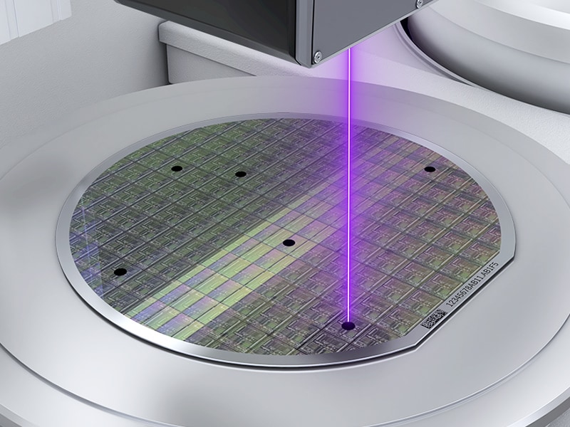
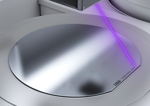
How Does a Wafer Marking Machine Work?
In a typical installation, a robot or wafer handling system presents wafers to a laser workstation or integrated marking module:
Wafer Presentation
- A robot retrieves a wafer from a FOUP/cassette and places it on a vacuum chuck or compatible stage.
- Orientation may use notch/flat detection and vision alignment.
Autofocus and Alignment
- 3 axis laser control dynamically adjusts focus position (Z direction) and field shape to accommodate variations in distance from the laser to the wafer.
- Vision assists with locating the designated mark field (edge, backside, or scribe line).
Marking
- The laser marks characters, logos, or 2D codes.
- Parameters favor low pulse energy, high repetition rate, and fast scanning to limit HAZ and debris.
Verification and Logging
- A vision inspection camera grades the mark (e.g., contrast, module integrity for 2D codes) and logs data to MES/traceability systems.
- If required, the system can re-mark or flag exceptions automatically.
The 3 axis autofocus feature of the MD-U2 helps sustain optimal focus even when wafer flatness varies lot-to-lot. Integrated quality validation cameras can immediately confirm readability and store images/grades, reducing downstream escapes and rework.
Laser Marking of Electronics & Semiconductors
Across electronics manufacturing, lasers are used for marking, cutting, drilling, coating removal, and more. In the semiconductor segment specifically, the demands are tighter due to:
- Extremely small features and characters
- Minimal heat-affected zone (HAZ) to protect device layers
- Cleanroom compatibility (low particles, no ink)
- High first-pass yield with automated inspection
- Traceable, standardized codes readable after downstream processing
UV laser markers are widely chosen for wafer and die identification because the shorter wavelength couples efficiently with many semiconductor and passivation materials while imparting less thermal load. This enables crisp, legible marks with low slag or redeposition—important for downstream lithography and packaging yield.
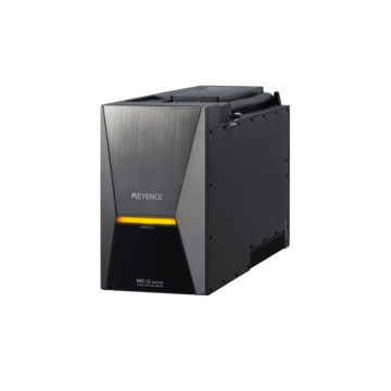
KEYENCE’s MD-U2 laser emphasizes low surface damage “cold” marking and integrates 3 axis autofocus to maintain mark quality during variations in part presentation to the laser. Combined with inline camera-based verification, this helps achieve stable markings with fewer adjustments and less operator intervention.
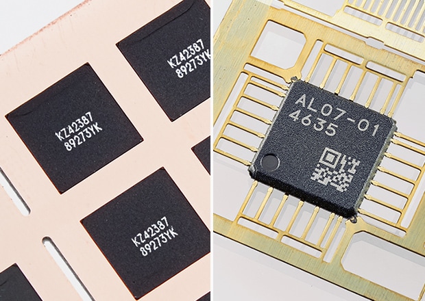
IC packages
Lead frames
Get detailed information on our products by downloading our catalog.
View Catalog

Laser Micromachining for Semiconductor Manufacturing
Beyond identification, lasers support a range of micromachining tasks on semiconductor parts and adjacent components:
- Thin-film ablation or passivation trimming
- Localized coating or resist removal
- Solder mask or polyimide windowing
- Marking and serialization on carriers, frames, and substrates
- Gentle texturing for optical or adhesion tuning
UV wavelengths are often preferred for these tasks because they enable fine features with limited thermal impact. While a dedicated micromachining cell may use different optics or motion, the same principles—short wavelength, precise focus, and debris mitigation—apply.
Clean Laser Marking of Wafers
“Clean” in this context means two things: low particle generation during the process, and a finished mark that does not shed debris or compromise downstream steps.
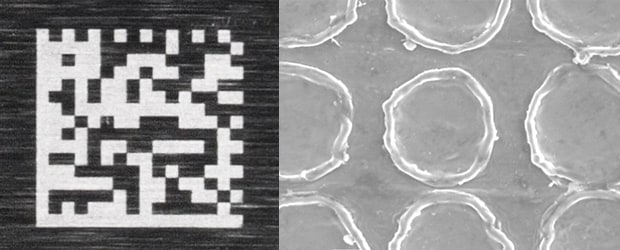
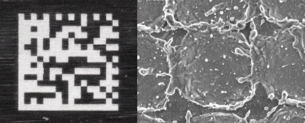
- UV “cold” marking vs. IR thermal marking: UV energy couples at the surface with less bulk heating, creating a smaller HAZ and less melting. IR can deliver excellent marks on many materials, but often imparts more heat, which can increase slag and recast on sensitive wafer surfaces. For wafers, UV’s low thermal load typically makes it the safer default.
- Autofocus for consistency: Wafer orientation variations to the laser, even a few millimeters, can shift the focal plane enough to result in a poorer quality mark. 3 axis autofocus stabilizes the focal point at the surface so the process stays within the low-damage window.
- Contamination control: Fume extraction, filtered enclosures, and well-defined airflow paths keep particles away from active areas. Short cycle times and low-damage cold marking reduce open-exposure intervals.
The MD U2 leverages a UV wavelength for low surface damage, with process stability enhanced by 3 axis autofocus. Pairing the marker with KEYENCE quality validation cameras enables immediate grading and image archiving of characters or Data Matrix/QR codes—supporting SPC, audits, and fast root-cause analysis if issues arise.
Practical Considerations and Best Practices
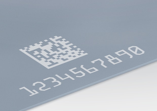
- Mark content: Most wafer IDs use human-readable text (lot/wafer number, date code) and, increasingly, 2D codes for robust, space-efficient traceability.
- Location choice: Backside or scribe line marks minimize interaction with active circuitry; confirm compatibility with your specific passivation and backside films.
- Parameter development: Start with low fluence (low laser energy on the surface), high rep-rate, fast scan speeds; iterate using microscopy and code grading to balance contrast vs. surface impact.
- Verification: Use inline cameras to measure contrast, edge quality, and code grade; log images plus results to your MES or database.
- Automation and throughput: Robot presentation with notch alignment and 3 axis autofocus reduces manual adjustments and supports consistent cycle times across shifts.
- Maintenance: Keep optics and filters clean; verify focus calibration and vision alignment on a defined interval to maintain Cp/Cpk (process capability).
UV Laser Marker
Fiber Laser Marker
IC Package (Epoxy): Marking with Reduced Engraving
Conventional
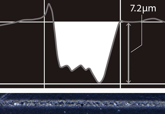
MD-U