Optical Comparator (Profile Projector)
Boosting Quality Control with Non-Contact Vision Measurement in PCB Manufacturing
Key Takeaways
- Use non-contact vision measurement for pre-assembly dimensional inspection with micron-level accuracy.
- Verify component placement and solder quality with combined XY and Z (confocal) measurements.
- Automatically record timestamped inspection data linked to serial/lot for traceability and root-cause analysis.
- Deploy multisensor systems (e.g., IM-X) to inspect thousands of locations faster, reducing rework and cycle time.
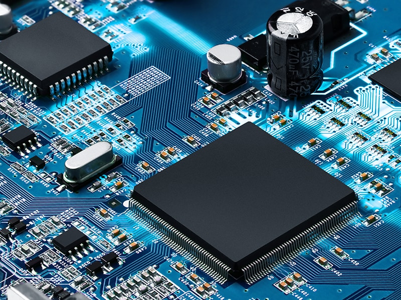
In PCB manufacturing, quality control isn't just a checkpoint—it's a mission-critical process that determines whether a product will perform reliably in the real world. As PCBs become more complex and densely packed, traditional inspection methods struggle to keep up. That's where non-contact vision measurement becomes a game-changer.
These systems offer unmatched measurement accuracy and efficiency by automating the dimensional inspection process, detecting errors early, and eliminating the need for manual measurements. Below, we explore three key stages in PCB dimensional inspection where non-contact vision systems are making a major impact.
1. Dimensional Inspection: Catching Flaws Before Assembly
Before components are even mounted, PCBs must meet strict dimensional tolerances. Tiny errors in trace width, pad size, or hole placement can lead to performance issues or outright failures. Manual tools like calipers or microscopes are slow, inconsistent, and not suitable for high-volume production.
Non-contact vision measurement systems solve this by using high-resolution cameras and software to automatically measure critical dimensions—without ever touching the board. They rapidly compare physical boards to nominal design values, ensuring early-stage accuracy before the assembly process begins.
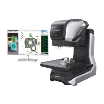
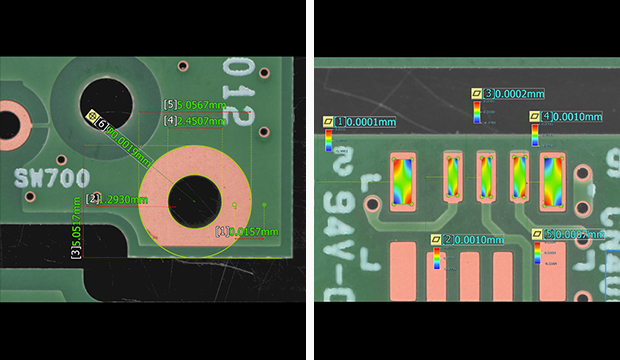
The KEYENCE IM-X system utilizes cameras accurate to .7 micron to inspect bare PCBs for rapid measurement. The system can identify where holes are off center, just enough to cause soldering defects during assembly. Because the issue is caught early, production can be paused and adjusted, saving time and costly rework.
By replacing manual checks with automated dimensional inspection, this approach delivers higher measurement accuracy and significantly boosts efficiency across the production line.
2. Assembly Verification: Ensuring Component Placement and Quality
Once components are mounted, ensuring proper placement and solder quality is essential. Errors like misaligned parts and tombstoning can escape detection in high-speed environments if relying on human inspection alone.
Enter non-contact vision measurement systems. These systems scan every board after component placement and soldering, detecting issues in real-time with extreme measurement accuracy.
In addition to non-contact vision measurement, the IM-X system is equipped with various Z height capabilities. A confocal laser can be used to collect Z data in a fraction of the time of traditional automated solutions and identify when components are lifting away from the board. Efficiency is with the IM-X by measuring XY and Z measurements in the same routine!
3. Post-Assembly Validation: Leveraging Automated Data Recording for Smarter Quality Control
After components are mounted and soldered, post-assembly inspection ensures the board meets all specifications before moving to final testing or shipment. While visual and functional inspections are essential, the ability to automatically record and analyze data is becoming just as important—especially in high-mix or high-volume environments.
Modern non-contact vision measurement systems don’t just inspect—they collect detailed, timestamped inspection data for every board. This automated data recording enables manufacturers to track trends, trace defects back to specific production batches, and maintain full quality documentation for audits or customer reports.
The IM-X automatically outputs measurement data—dimensional measurements, defect locations, and pass/fail status—Can be recorded and linked to the board’s serial number/lot number. When a client later reports an issue, engineers can instantly pull up the board’s full inspection history to identify root causes and verify compliance.
This level of traceability improves long-term accuracy in quality reporting and offers significant efficiency gains by reducing manual paperwork and guesswork. With automated data capture, quality teams can focus on optimization instead of documentation.
Conclusion: Smarter Inspection, Better Results
Non-contact vision measurement is revolutionizing how PCB manufacturers approach quality control. From ensuring dimensional integrity to validating component placement and automating post-assembly data recording, these systems improve inspection speed, traceability, and confidence at every stage.
By embracing this technology, manufacturers achieve higher accuracy, greater efficiency, and a more intelligent approach to quality—ensuring their products meet the expectations of both regulators and customers.
Looking to Implement an Optical Inspection System for PCBs?
If you’re ready to integrate PCB inspection for your facility, KEYENCE can help. We specialize in multisensor measurement systems for automated PCB inspection.
KEYENCE’s IM-X Series can inspect 5,000 locations on multiple PCBs simultaneously— meaning that inspection tasks are shortened in time and cost per inspection.
If you are ready to implement PCB inspection equipment, contact KEYENCE today.