3D Optical Profiling Microscope
3D Optical Profiling Microscope
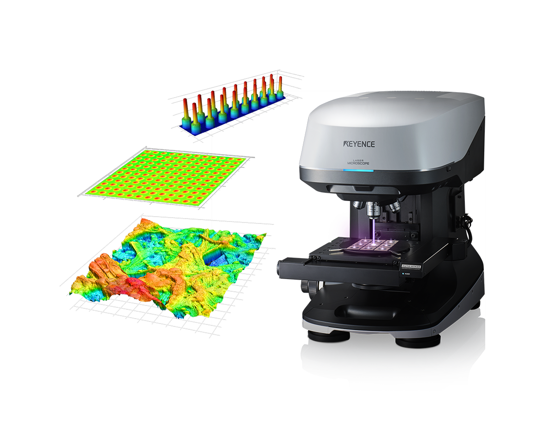
A non-contact 3D optical profilometer designed to capture SEM-like images and measure surface roughness and texture, 3D topography, and film thickness on virtually any material with sub-nanometer resolution. The VK-X Series gives engineers and researchers the surface measurement clarity that other measurement systems simply can't match.
Product Lineup
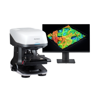
The VK-X4000 Series 3D Optical Profiling Microscope combines laser confocal, white light interferometry, and focus variation methods into a single metrology system, enabling highly accurate, non-contact measurements on nearly any material and surface geometry. Its newly-developed multi-point measurement function further streamlines the analysis process by automating measurements across multiple locations and samples—eliminating complex setup or programming while delivering greater usability, throughput, and repeatability.
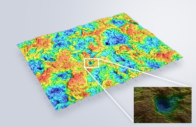
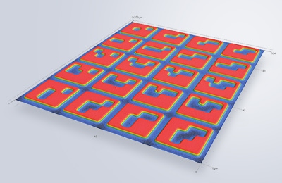
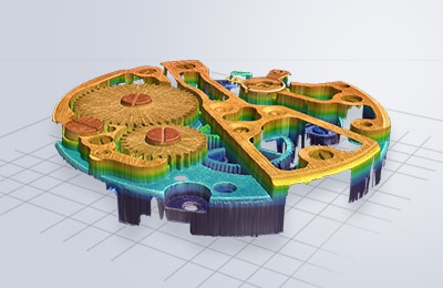
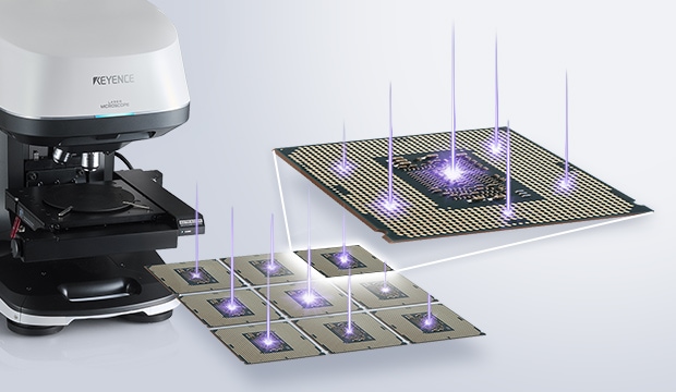
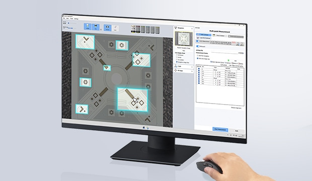
A 3D optical profiling microscope is an instrument that captures 3D data on the surface of a target, typically for measuring surface roughness. 3D optical profiling microscopes can use white light, a laser, or other methods as a means to capture data. Conventionally, stylus probes made of diamond were used for profiling surfaces; however, most industries are shifting to optical systems due to the surface being scratched and potentially damaged when using a physical stylus probe.
Common applications for a 3D optical profiling microscope include quantifying surface roughness and texture, micro-feature profiling and film thickness measurement, and defect and material analysis.
Benefits of 3D Optical Profiling Microscopes
3D measurement systems fall into two main categories: contact and non-contact. Contact systems use a probe or stylus that physically touches the surface being measured, which introduces several limitations. They can damage delicate surfaces, cannot reliably measure viscous or adhesive materials, and cannot resolve surface features smaller than the tip of the stylus.
The VK-X4000 Series is a non-contact system that overcomes each of these limitations. Because nothing touches the sample, there is no risk of surface damage and no difficulty measuring adhesive or viscous materials. And with a laser beam spot radius of just 0.2 micron, the VK-X4000 Series can resolve features far smaller than any stylus tip can reach.
Imaging systems tend to sit at two extremes. Optical microscopes are the general standard, but they suffer from a shallow depth-of-field and limited spatial resolution (approximately 500 nm). At the other end, SEMs deliver extremely high resolution and magnification, but they produce only monochrome images, cannot accommodate larger objects without destroying them, are difficult to operate, and require samples to be coated in a conductive material and scanned within a vacuum.
KEYENCE's 3D Optical Profiling Microscope bridges the gap between the two. Using a white light source and a laser source together with a focus-stacking algorithm, the VK-X4000 Series captures fully-focused images — overcoming the shallow depth-of-field of optical microscopes — and achieves a spatial resolution of 120 nm, well beyond their ~500 nm limit. It also delivers what SEMs cannot: high-definition color images at up to 28800× magnification, with no sample preparation, no conductive coating or vacuum, and non-destructive imaging of even large objects.
Most measurement systems rely on a single measurement principle. That works for some targets, but every principle has blind spots, so other targets demand a different system entirely. White light interferometry, for example, struggles with very rough surfaces or steep angles, forcing the user to switch to a laser confocal microscope to get accurate data. Covering a wide range of targets can therefore mean owning several separate instruments.
KEYENCE's 3D Optical Profiling Microscope removes that trade-off. By combining laser confocal scanning, white light interferometry, and focus variation in a single system, the VK-X4000 Series can measure nearly any target, from the millimeter scale down to the micrometer and nanometer scale. What would typically take three different measurement systems, KEYENCE's integration of three measurement principles accomplishes with one device, no matter the material or shape.
Stylus-Based Profilometers for Roughness Measurement
With contact-type surface roughness instruments, a stylus tip makes direct contact with the surface of a sample. The detector is equipped with a stylus, which traces the surface of the sample and electrically detects the vertical motion of the stylus.
The electrical signals go through an amplification and digital conversion process to be recorded.
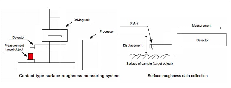
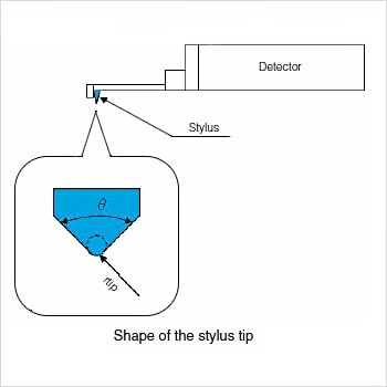
To precisely measure delicate shapes and roughness with a stylus profilometer, the radius of the stylus tip must be as small as possible with low contact pressure.
Styluses are made of sapphire or diamond, and their tip radius is usually about 10 µm 0.39 mil or smaller. A conical shape with a ballpoint tip is considered ideal for a stylus.
Tip radius: r tip = 2 µm 0.08 mil, 5 µm 0.20 mil, 10 µm 0.39 mil
* Cone taper angle: 60º, 90º
* Unless otherwise specified, cones have a 60º taper.
Stylus Profilometer Characteristics
Stylus-based roughness gauges provide reliable measurements because they directly touch the sample. However, direct contact to a sample often has many disadvantages as outlined below.
Advantages
- Clear wave profile
- Capable of long-distance measurement
Disadvantages
- Stylus wear
- Measuring pressure can cause scratches on the sample surface
- Inability to measure viscous samples
- Measurement limited by radius of stylus tip
- Time-consuming
- Difficulties in positioning and identification of subtle measuring points
- Requires sample cutting and processing for tracing by the detector
Non-Contact 3D Optical Profilometers for Roughness Measurement
A 3D optical profilometer uses light instead of a stylus for measuring a surface. There are several types of these instruments, such as laser confocal microscopes and white light interferometers, and each can vary depending on the principle(s) used. There are also a variety of stylus profilometers that have been adapted into non-contact systems by replacing the probe with optical sensors or other devices. We will use KEYENCE's 3D Optical Profiling Microscope, the VK-X4000 Series, as an example to explain the principles of the different technologies available.
A 3D optical profiling microscope integrates three different measurement principles - laser confocal, interferometry, and focus variation - to accommodate and measure any type of surface. Let's take a look at each of these technologies to better understand how they work.
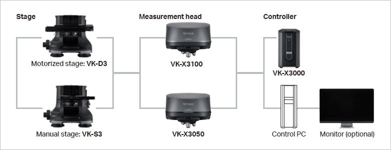
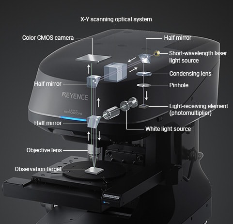
With KEYENCE's VK-X4000 Series, a galvanometric scanner is embedded in the measurement unit. The laser light source scans across the surface of the target in the X and Y directions and acquires the surface data.
The scanning principles are explained below.
1. Industrial Laser Confocal Measurement
What it is:
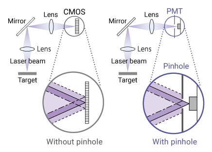
An industrial laser confocal microscope uses focused laser light and specialized optics to measure surface topography without physical contact. The confocal design places a pinhole before the detector, blocking scattered light from areas outside the focal plane. Only light reflected from the exact focal point passes through, creating sharp height discrimination.
This configuration delivers two benefits simultaneously. First, it produces exceptionally clear images by eliminating optical noise. Second, by scanning the laser across a surface and tracking intensity changes, the system builds accurate 3D height maps. Manufacturing facilities use these tools for everything from roughness analysis on machined parts to quality verification of coated surfaces.
Principle:
Laser microscopes utilize a specialized optical system consisting of a laser light source, objective lens, half mirror, pinhole, and laser light receiving element (PMT) to perform both magnified observation and surface shape analysis.
In this system, laser light from the source is concentrated by the objective lens onto the measurement target positioned at the focal point. The reflected light from the target surface then passes back through the objective lens and is focused once more at a precisely positioned pinhole directly in front of the light receiving element.
When the target is correctly positioned at the focal point, the reflected laser light concentrates into a tight beam that passes completely through the pinhole, allowing all of the light to reach the receiving element. However, when the target is out of focus, the laser light spreads and becomes less concentrated, causing the pinhole to block a portion of the reflected light and reducing the intensity received by the detector.
By monitoring the intensity of this reflected light, laser microscopes can accurately determine whether the sample is at the focal position. This optical configuration—featuring a pinhole positioned before the light receiving element—is known as a confocal optical system, and its detection method is called the confocal principle.
How laser scanning technology captures 3D data:
Laser microscopes employ various scanning techniques to acquire surface data, each offering distinct trade-offs between speed, accuracy, and versatility. The three most common approaches are the Galvano scanner, acousto-optic device (AOD), and Nipkow disk methods.
Galvano scanner method:
This method uses servo-controlled mirrors to direct laser light across the sample surface. The mirrors, mounted at the ends of servo motors, rotate to precisely adjust their angles and sweep the laser beam in both X and Y directions. This mechanical approach delivers high-quality data with excellent accuracy, though the physical movement of the mirrors results in slower scanning speeds.
Acousto-Optic Device (AOD) method:
The AOD method takes a fundamentally different approach by using light diffraction rather than mechanical movement. An electric signal applied to a piezoelectric element generates ultrasonic waves within a glass acousto-optic medium. These waves diffract the passing laser light, effectively steering the beam across the sample. This enables significantly faster scanning speeds compared to mechanical methods, though the data quality can suffer from distortion artifacts.
Nipkow disk method:
This technique employs a rotating disk containing spirally arranged pinholes to create multiple scanning beams simultaneously. As the disk spins, numerous light beams pass through the pinholes and sweep across the sample surface in parallel. This parallel scanning approach maintains relatively high data quality while improving speed, but the method struggles with samples that have low reflectivity, as the divided light intensity may be insufficient for clear detection.
2. White Light Interferometry
Principle:
White light interferometry captures 3D shape data through the observation of light interference patterns using an image sensor, such as a CMOS. Using an interference objective lens with a built-in reference mirror, white light from an LED or other light source is used to illuminate the reference mirror and the target (measurement surface). The light reflected from each object interferes with one another, and the interference pattern appears as contour lines at each half wavelength. This corresponds to the shape of the target surface with respect to the reference mirror. The interference stripes are then captured by the image sensor, and processing is used to determine the 3D shape of the target.
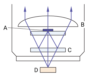
A: Reference mirror, B: Objective lens, C: Beam splitter, D: Sample
3. Focus Variation
Principle:
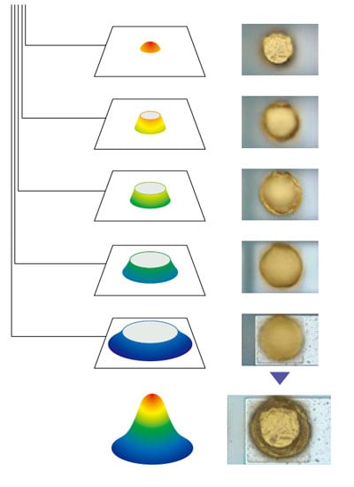
Focus variation determines surface height by analyzing how image sharpness changes at different focal positions. The technique uses a high-resolution image sensor to identify the precise focal point for each pixel across the sample surface.
The measurement process involves capturing a series of images while incrementally moving the lens in the Z direction. As the lens shifts through different heights, various portions of the sample come into and out of focus. The key to detection lies in analyzing the brightness contrast between adjacent pixels in each image.
When an area is in sharp focus, edges and details appear crisp, creating strong brightness differences between neighboring pixels. Conversely, when that same area is out of focus, the image becomes blurred—causing these brightness differences to diminish as pixel values blend together.
By tracking where the brightness contrast reaches its maximum value for each pixel location, the system identifies the exact lens position where that point is in sharpest focus. This focal position corresponds directly to the surface height at that location, allowing the system to construct a complete 3D height map of the sample.
Non-Contact 3D Optical Profiling Microscope Characteristics
In addition to the points that have already been explained, the characteristics of non-contact types can be summarized as shown below.
Advantages
- No sample surface damage
- Able to measure smaller changes than stylus-type systems
- Quick measurements
- Simultaneous observation of surface image and height profile
- Able to acquire high-definition, fully-focused images that rival those of SEMs
3D Optical Profiling Microscope Case Studies
Surface roughness measurement
Surface roughness has many standardized parameters; the more the parameters, the more complicated measurement becomes, which tends to mean more time spent to complete an evaluation. Quantification on its own is not sufficient to make a judgment, and pass/fail tests and quality control can be challenging. KEYENCE’s VK-X4000 Series 3D Optical Profiling Microscope can scan the surfaces of targets with high definition and provide quantitative 3D measurements. The measurement results can be subjected to pass/fail tests by comparing them across multiple samples using 42 roughness parameters. Surface roughness is quantified, and roughness distribution can be visualized in graphs, which enables instantaneous quantification of differences in material, finish, texture, feel, and other appearance characteristics.
SEM-like imaging
The VK-X4000 Series is equipped with a color CMOS camera and a 16-bit PMT for capturing the returned laser light. Due to the increased resolution when using a laser over white light, the VK-X4000 Series is capable of capturing high magnification images with a higher resolution than standard optical microscopes. With a maximum achievable magnification of 28800×, the VK-X4000 Series can capture high-resolution color images that rival an SEM. Additionally, no sample prep is required when using the VK-X4000 Series, so images can be captured instantaneously.
Measuring large targets
Generally, 3D optical profiling microscopes cannot measure targets that cannot be placed on the XY stage. However, a VK-X4000 Series 3D Optical Profiling Microscope is structured so that it is possible to separate the microscope into a measuring head and base. This allows for the measurement head to be integrated with larger stages, allowing for a nearly limitless measurement range.
Touching a sample changes it. Stylus probes leave microscopic scratches. Soft materials deform under probe pressure. Adhesive surfaces grab the tip and contaminate subsequent measurements. Non-contact profiling solves all three problems by keeping optics away from the part.
This matters especially for finished surfaces. Coated components, polished optics, and painted parts can all be measured without risk of damage. You verify quality without creating the defects you're checking for. The same principle applies to fragile samples, where even minimal contact force would crack or deform the structure.
A 3D optical profiling microscope quickly completes full-area scans, capturing data that would take hours with a stylus probe. You get complete surface characterization instead of a handful of line profiles. This comprehensive view reveals defects that traditional sampling methods miss entirely.
The technology also eliminates operator dependency. Stylus measurements vary based on probe pressure, trace direction, and point selection. Different technicians produce different results on identical parts. 3D optical profiling microscopes remove these variables. The measurement parameters stay consistent regardless of who runs the system, giving you reliable data for process control and trend analysis.
Traditional 3D surface profilers typically employ a single measurement method, whether that be a stylus probe, single-point laser, or white light. Each method has its advantages in regard to speed, resolution, data volume, or material type; however, only using a single measurement principle can create serious limitations when it comes to those that have a variety of samples to measure and analyze.
A 3D optical profiling microscope incorporates three unique measurement methods - laser confocal, white light interferometry, focus variation - in order to combine the advantages of all of these systems into a single platform. Users have the ability to capture high-resolution images, measure with sub-nanometer resolution, rapidly scan an entire area, and measure on any type of material or topography - including steep slopes or highly-curved surfaces.
Standard optical microscopes struggle with depth of field. Bring one feature into focus, and everything above or below it blurs. A 3D optical profiling microscope uses confocal optics to reject out-of-focus light, producing sharp images across height variations that would overwhelm conventional systems.
The result looks similar to SEM imagery but in full color and without sample preparation. You see fine surface details at magnifications up to 28800× while simultaneously collecting quantitative height data. This dual capability supports both visual inspection and dimensional verification in a single scanning cycle, streamlining quality workflows that previously required multiple instruments.
Related Products
Industrial confocal microscopes incorporate a pinhole in front of the light-receiving element to block ambient and out-of-focus light. This allows the microscope to use the position that has reflected the most intense light as the true height. The following section describes the individual steps of the detection process of the KEYENCE 3D Optical Profiling Microscope.

This website provides information on how a 3D optical profiling microscope can be used to quantify surface texture and roughness, including relevant terminology, roughness parameter definitions, and the pros and cons of different measuring instruments.
Frequently Asked Questions About 3D Optical Profiling Microscopes
Unlike SEMs and conventional microscopes that require extensive training and expertise, the VK-X4000 Series 3D Optical Profiling Microscope is designed for intuitive operation by users of any skill level.
The key to this accessibility is the AI-Scan function, which automates the entire data acquisition process. Advanced algorithms intelligently adjust multiple scan settings in real-time, eliminating the need for manual optimization. Operators simply place the sample on the stage and press the measure button—the system handles the rest.
This automation delivers consistent, accurate results regardless of the operator's background or experience. By removing the dependency on specialized skills, the VK-X4000 Series provides access to high-quality measurements across your organization and eliminates the need for lengthy training programs.
The maximum magnification provided by VK-X4000 Series 3D Optical Profiling Microscope is 28800× (with a 23-inch monitor full display). We provide a wide-ranging lineup of dedicated lenses from 2.5× to 150×, all of which undergo rigorous inspection before being shipped. Long working distance lenses are available for measuring targets with large height changes and high aspect ratios.
No—the VK-X4000 Series employs a flexible company license system that removes this limitation entirely. The software can be installed and used on multiple computers throughout your organization at no additional cost, providing unprecedented access and collaboration capabilities.
This licensing approach enables true operational flexibility. Users can work remotely from home, access data from different office locations, or even review measurements while traveling. The multi-computer capability also facilitates instant data sharing among team members, accelerating project workflows and enabling faster decision-making across your organization.
A 3D optical profiling microscope performs non-contact 3D surface measurement, roughness analysis, and high-magnification imaging across manufacturing and research applications. Common uses include measuring machined surface finish, inspecting coating thickness, analyzing wear patterns, and quantifying microscopic height changes in surface topography.
It focuses a laser beam onto the sample surface and detects reflected light through a pinhole that blocks out-of-focus signals. By scanning this focused spot across the surface and tracking intensity changes, the system determines height at each location and builds a complete 3D profile.
A 3D surface profiler typically uses a stylus or single-point sensor to trace surface profiles sequentially. A 3D optical profiling microscope captures full-field data simultaneously through area scanning, providing faster measurement with visual imaging capability. Laser systems also avoid contact-related damage and measure complex geometries that probes cannot reach.
Laser scanning delivers both speed and precision without touching the sample. The technique captures complete surface topography in seconds, handles steep angles and complex shapes that other methods simply can’t, and provides quantitative height data alongside high-resolution images. For detailed information on laser scanning principles and capabilities, visit KEYENCE's laser scanning confocal microscope resources.

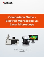
A must-read document for anyone using a scanning electron microscope (SEM). This guide introduces the full extent of the capabilities of the latest 3D surface profilers, using many measurement and observation images. A rich source of information that helps you understand and solve problems you may experience with an SEM.