Machine Vision
How Machine Vision Applications in Semiconductor Manufacturing Boost Quality Control
Manufacturing semiconductors is a complex process consisting of wafer fabrication, photoresist coating, lithography, etching, ion implantation, and other processes. Incorporating machine vision in semiconductor manufacturing helps with faster chip production, boosting the efficacy and precision of operations and giving manufacturers a competitive advantage.
Introduction to Machine Vision in Semiconductor Manufacturing
Semiconductor manufacturing refers to how integrated circuits (IC) are built into modern electronic devices. Many modern conveniences, including computers, wouldn't have been possible without integrated circuits.
Wafer creation, circuit construction, and packaging are three major stages in the fabrication process. Once raw materials such as silicon or compounds for the fabrication process have been sourced, gases like oxygen, nitrogen, and argon, amongst other chemical reactions, are used to create the correct environment that will shape the semiconductor's electrical properties.
Equipment like dice machines is utilized to cut a wafer into chips or dies. Probing machines are used to test how well-functioning individual chips are before packaging. Grinders and edge-shaping tools are other equipment used.
When manufacturing these chips, all the parts that make up the semiconductor must be properly assessed for factors such as alignment, defects, and traceability. Inspection precision is even more critical in modern and sophisticated integrated circuits. This is why machine vision applications in semiconductor manufacturing play a key role.
Overview of Semiconductor Manufacturing
Semiconductor manufacturing is a highly precise, multi-step process that transforms raw silicon into functional integrated circuits. The process begins with creating ultra-pure silicon ingots, which are sliced into thin wafers that serve as the foundation for chip production. These wafers undergo dozens of fabrication steps, including cleaning, oxidation, photolithography, etching, and doping to create the intricate circuit patterns.
Modern semiconductor factories operate in cleanroom environments where even microscopic particles are strictly controlled, as contamination as small as 0.5 microns can render chips defective. Repeated stacking is used in the fabrication process; each chip can have up to 100 layers of various materials, all of which must be precisely aligned with one another. Since feature sizes in sophisticated semiconductors are now measured in nanometers, this procedure requires an incredible level of precision.
After fabrication, completed wafers undergo electrical testing before being separated into individual dies, which are then packaged to protect the circuits and enable connection to external devices. Rapid quality control is crucial to spotting problems early and reducing expensive mistakes that could affect entire production batches, as the entire manufacturing cycle from raw silicon to completed chips normally takes 10–12 weeks.
The economics of semiconductor manufacturing has driven significant technological advancements in process control and automation. With modern fabrication facilities costing upwards of $20 billion to construct, manufacturers must maximize efficiency at every stage. Each 300 mm wafer can contain hundreds or even thousands of individual chips, with high-end processors potentially worth over $100,000 per wafer at the final test.
Advanced systems that can identify submicron flaws in real time have become popular regardless of the machine vision application in semiconductor manufacturing. This enables quick process adjustments and drastically lowers scrap rates. Automated inspection is becoming more important to sustaining profitability as chip designs continue to grow more sophisticated while shrinking in size.
The Importance of Quality Control in Semiconductor Manufacturing
To speed up production times, IC manufacturers need systems for alignment, defect, and traceability inspections. Three top benefits of machine vision in semiconductor manufacturing include:
Alignment
Silicon wafers, which form the foundation of ICs, need to be manufactured and placed on top of each other in layers. Every single layer must align precisely. The orientation of a wafer notch, the tiny cut intentionally made on the edge of a silicon wafer for alignment purposes, is then checked. Using traditional inspection systems is slow and bulky, especially when it comes to accurately detecting a notch in transparent wafers.
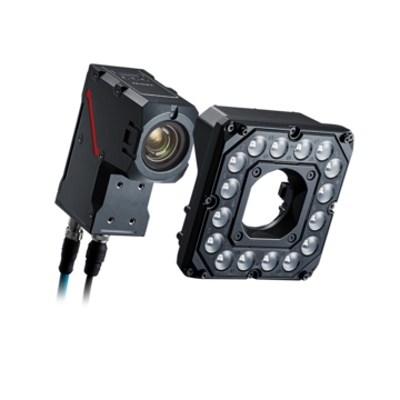
KEYENCE vision systems with built-in AI help improve silicon wafer alignment due to the advanced and proprietary functions they feature. The AI capability is a deep learning tool that trains on a large data set of images to accurately recognize dots on even transparent wafers.
Defect Detection
Catching defects early during production helps improve the production line yield rate per wafer by minimizing manual inspection and rework. Because wafers are stacked, each layer must be inspected before being deposited on the other to identify defects.
Without accurate inspection systems, classifying real defects from allowable cosmetic flaws becomes challenging, leading to rework and waste. Accurate defect detection and cost savings are other reasons to use machine vision in semiconductor quality control efforts.
Identification and Traceability
Wafers, wafer carriers, dies, lead frames, integrated circuits, and other semiconductor components can be counterfeited. These components carry alphanumeric characters (for tracking and a human-readable format) and identification codes (for identification and a machine-readable format). Instead of using conventional methods to read codes and characters, vision systems make decoding easy and error-free even when codes are damaged or are difficult to read.
Common Quality Control Challenges
Like many other production processes, manufacturing semiconductor components comes with its own set of unique challenges.
Yield
The complexity of the manufacturing process makes achieving a high yield, i.e., more good chips per wafer produced, challenging. Fortunately, accurate defect detection helps identify and eliminate defective wafers, helping maximize the percentage of good chips. Machine vision systems can improve yield rates by 3-5% through early detection of process drift and pattern defects that might otherwise go unnoticed until electrical testing.
Contamination
Chemicals and foreign materials can contaminate wafers during production. Even the tiniest of particles can cause defects, leading to malfunctions of produced circuits. Advanced semiconductor processes now work at the 5 nm scale and below, where even particles smaller than 0.1 microns can cause defects. Vision system inspection can detect these invisible contaminants by analyzing light refraction patterns that reveal surface anomalies undetectable to the human eye.
Environmental Factors
Accurate temperature must be maintained to achieve consistency in the production of every part that goes into integrated circuits. Temperature variations as small as ±0.5°C can cause dimensional changes that affect lithography precision and chemical reaction rates. Modern fabrication facilities integrate real-time environmental monitoring with industrial vision systems. These allow automated compensation for micro-variations in conditions that would otherwise impact quality.
Wafer Inspection
Using the wrong inspection systems can make wafer inspection difficult. The inspection system used must identify cracks, contamination, and scratches while making allowance for cosmetic flaws. The latest wafer vision system inspection technologies combine bright-field, dark-field, and phase contrast imaging to achieve defect sensitivity while maintaining throughput.
Machine Vision Applications in Semiconductor Manufacturing
The use of machine vision helps in semiconductor fabrication. Vision systems can check for wafer alignment, detect a wide range of defects, and enable accurate identification and tracing of wafers and chips.
Inline 3D Inspection
Using vision products that can perform inline 3D inspection provides significant benefits to the production of wafers, chips, and PCBs. By identifying defects early in the production process, these vision systems can reduce scrap rates and improve yields. 3D machine vision is also used in semiconductor manufacturing to improve defect detection. 3D vision systems create three-dimensional data, including depth profiles, which help uncover voids, undercuts, and delamination.
Line Scan Technology
Line scan technology is also used in semiconductor production. These cameras are especially useful because they can perform accurate inspection of defects and contamination even on uneven surfaces. These specialized cameras deliver exceptionally high-resolution imaging, enabling accurate inspection of defects. By capturing data one line at a time as products move through production, line scan systems can detect microscopic flaws while maintaining throughput requirements.
AI-Powered Vision Systems
Vision system inspection can check for wafer alignment, detect a wide range of defects, and enable accurate identification and tracing of wafers and chips. Modern AI-powered industrial vision systems leverage deep learning algorithms to distinguish between actual defects and acceptable variations, drastically reducing false positives. These intelligent systems continue improving over time as they process more image data, leading to increasingly accurate inspections without requiring explicit reprogramming.
The Benefits of KEYENCE Machine Vision Systems in Semiconductor Manufacturing
High-Speed and Accurate Inspections
A KEYENCE vision system for manufacturing delivers unprecedented inspection speeds without compromising accuracy, with specialized hardware capable of processing up to 64-megapixel images in milliseconds. The systems can capture entire PCBs in a single shot while simultaneously performing multiple inspection tasks, including component presence verification, dimensional measurement, and surface defect detection. This high-throughput capability allows semiconductor manufacturers to maintain production speeds while achieving 100% inspection coverage.
Enhanced Efficiency
KEYENCE vision systems drastically cut labor expenses and human error by automating inspection procedures that previously needed manual intervention. Consistent quality is guaranteed throughout production runs of any length of time because of the system's capacity to function constantly without becoming tired or losing focus. Additionally, integrated reporting tools provide real-time production metrics that help identify bottlenecks and optimization opportunities throughout the manufacturing process.
Comprehensive Traceability and Quality Control
KEYENCE vision systems establish complete component traceability through robust code reading capabilities that function even with partially damaged or low-contrast markings. A thorough audit trail is produced for regulatory compliance and process enhancement by automatically recording the timestamp data for each inspection result. Tracking pinpoints the exact time and location of production process flaws, enabling manufacturers to promptly isolate and resolve quality concerns.
Transform Your Semiconductor Manufacturing with KEYENCE AI-Powered Vision Systems
KEYENCE AI vision systems for the semiconductor and electronics manufacturing industry help enhance operations. Our AI-powered vision system uses deep learning techniques to improve defect detection accuracy, read codes for traceability, and alignment checking. It can train on extensive image data to learn what is classified as defects and what is permissible as cosmetic flaws.
Our vision systems also enable high-speed and accurate inspections of various semiconductor components. A 64-megapixel camera can capture the entire PCB in one image shot, enabling simultaneous semiconductor inspections such as product measurement and differentiation.
To learn more about how our AI-powered vision can bring benefits to semiconductor manufacturing, contact us today.

FAQs
How Does Machine Vision Improve Alignment in Semiconductor Manufacturing?
A machine vision system for manufacturing provides precise alignment of wafer layers by detecting microscopic positioning markers with sub-micron accuracy. The systems use advanced algorithms to compensate for thermal expansion and other variables, ensuring each layer is perfectly positioned relative to previous layers even at high production speeds.
Why Is Line Scan Technology Used in Semiconductor Production?
Line scan technology offers superior resolution for inspecting moving components at high speeds without motion blur. This technology is particularly valuable for examining continuous materials or large surfaces where small defects might go undetected with traditional area scan cameras.
What Industries Benefit Most From KEYENCE Machine Vision Systems?
KEYENCE industrial vision systems aid the automotive, pharmaceutical, and consumer electronics industries in addition to the semiconductor manufacturing sector. Utilizing the same fundamental technology, these various applications tackle industry-specific inspection issues in a variety of production settings.
How Does KEYENCE Ensure the Quality of Its Vision Systems for Semiconductor Manufacturing?
KEYENCE maintains quality standards through comprehensive testing for any machine vision application in semiconductor manufacturing environments. Each system undergoes calibration verification and performance validation before shipping, with ongoing support including regular firmware updates that incorporate new inspection algorithms and performance enhancements.
How Does AI Contribute to KEYENCE Machine Vision Systems?
AI enhances KEYENCE vision systems through deep learning algorithms that can distinguish between actual defects and acceptable variations. These intelligent systems improve over time as they process more data, learning to recognize complex patterns without explicit programming while reducing false positives and improving inspection accuracy.