Vision Systems
CMOS and Image Processing Solutions
Key Takeaways
- CMOS sensors convert light to voltage at each pixel, enabling faster readout and lower power.
- Image processing detects defects by comparing local pixel regions against thresholds and patterns.
- Pixel count and density determine detectable feature size; excessive resolution slows processing.
- CCDs deliver more uniform, low-noise output and better long-exposure performance; CMOS favors speed and integration.
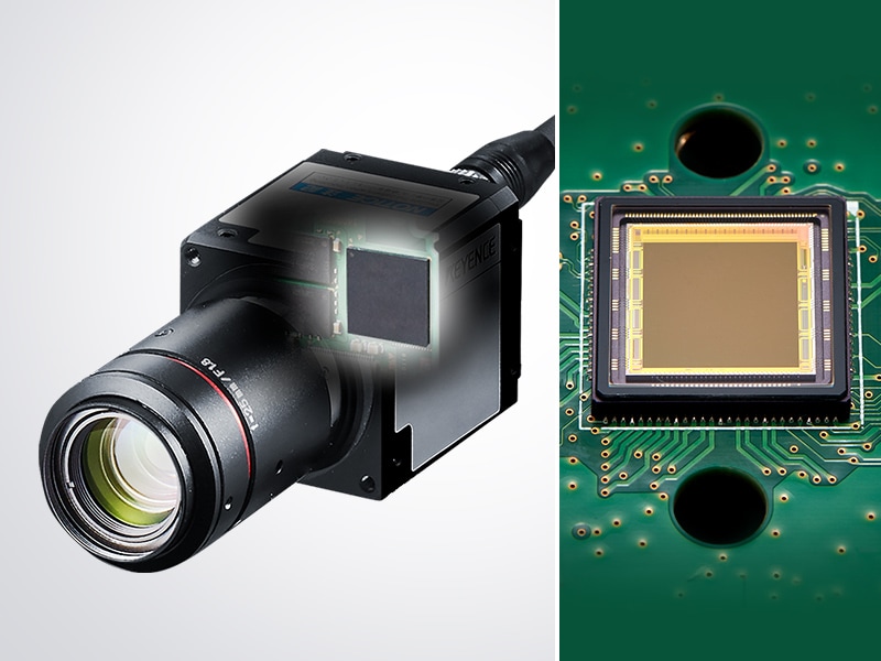
Modern machine vision systems, like those from KEYENCE, rely on precise image capture and reliable data to be interpreted that support automated inspection, measurement, and identification tasks. At the center of these image processing systems are image sensors that convert light into usable digital information. Understanding how complementary metal-oxide-semiconductor (CMOS) sensors function and how their data is processed is a core part of vision system basics and how they work.
How CMOS Sensors Work: From Light to Pixel Data
A CMOS image sensor converts incoming light into electrical signals that can be processed by a vision controller. The surface of the sensor is made up of a grid of pixels, each containing a photodiode and necessary circuitry. Light passes through a lens and hits the sensor, and each pixel responds by generating an electrical response. The intensity of the response is based on the signal it receives.
Unlike older sensor architectures that rely on shared readout paths, CMOS sensors perform their signal conversion directly at the pixel level, and each pixel converts the light into voltage on a local level, which allows for multiple pixels to be read together. This supports higher read-out speeds and also helps lower power consumption, making CMOS technology a standard across most machine vision systems.
Once the pixels have responded, the sensor outputs digital image data that represents brightness values from across the field of view. The resulting image is a structured set of numerical data that can then be evaluated and analyzed by image processing systems.
CCD Image Sensor
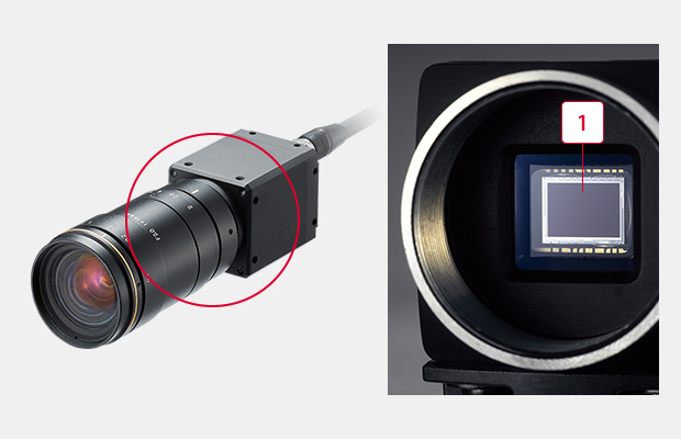
A digital camera has almost the same structure as that of a conventional (analog) camera, but the difference is that a digital camera comes equipped with an image sensor called a CCD. The image sensor is similar to the film in a conventional camera and captures images as digital information, but how does it convert images into digital signals?
-
1CCD image sensor
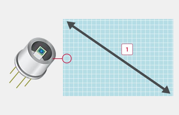
The CCD stands for a Charge Coupled Device, which is a semiconductor element that converts images into digital signals. It is approx. 1 cm in both height and width, and consists of small pixels aligned like a grid.
When taking a picture with a camera, the light reflected from the target is transmitted through the lens, forming an image on the CCD. When a pixel on the CCD receives the light, an electric charge corresponding to the light intensity is generated. The electric charge is converted into an electric signal to obtain the light intensity (concentration value) received by each pixel.
-
11/1.8-inch (approx. 9 mm)
This means that each pixel is a sensor that can detect light intensity (photo diode) and a 2 million-pixel CCD is a collection of 2-million photo diodes.
A photoelectric sensor can detect presence/absence of a target of a specified size in a specified location. A single sensor, however, is not effective for more complicated applications such as detecting targets in varying positions, detecting and measuring targets of varying shapes, or performing overall position and dimension measurements. The CCD, which is a collection of hundreds of thousands to millions of sensors, greatly expands possible applications.
Use of Pixel Data for Image Processing
This section of the page briefly details the method in which light intensity is converted into usable data by each pixel and then transferred to the controller for processing.
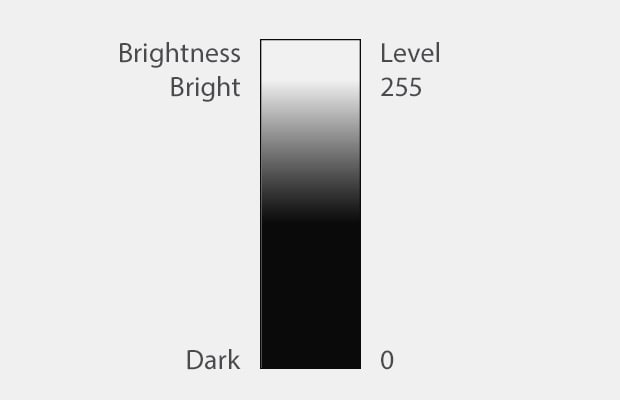
Image of 256 brightness levels
Individual Pixel Data (In the Case of a Standard Monochrome Camera)
In many image sensors, each pixel transfers data in 256 levels (8 bit) according to the light intensity. In monochrome (black & white) processing, black is considered to be “0” and white is considered to be “255”, which allows the light intensity received by each pixel to be converted into numerical data. This means that all pixels of a CCD have a value between 0 (black) and 255 (white). For example, gray that contains white and black, exactly half and half, is converted into “127”.
An Image Is a Collection of 256-Level Data
Image data captured with a CCD is a collection of pixel data that make up the CCD, and the pixel data is reproduced as a 256-level contrast data.
As in the example below, image data is represented with values between 0 and 255 levels per pixel. Image processing is processing that finds features on an image by calculating the numerical data per pixel with a variety of calculation methods, as shown below.

Raw image

When the image on the left is represented with 2500 pixels

The eye is enlarged and represented as 256-level data.
The eye has a value of 30, which is almost black, and the surrounding area has a value of 90, which is brighter than 30.

Example: Stain / Defect Inspection
The inspection area is divided into small areas called segments and the average intensity data (0 to 255) in the segment is compared with that of the surrounding area. As a result of the comparison, spots with more than a specified difference in intensity are detected as stains or defects.
The average intensity of a segment (4 pixels x 4 pixels) is compared with that of the surrounding area. Stains are detected in the red segment in the right example.
Advanced Image Processing Techniques for Defect and Stain Detection
Image processing starts once pixel data is captured and transferred. In industrial vision systems, this data helps detect product changes that indicate errors. Defect and stain detection typically compares local pixel regions to surrounding areas to identify deviations.
Rather than interpreting an image as a whole, image processing systems divide the image into smaller regions. Each is evaluated mathematically using brightness values and spatial relationships. Any differences that go beyond a pre-defined threshold are flagged as potential defects, and more advanced image processing techniques may incorporate adaptable thresholds or pattern-based analysis to account for natural variations. These methods help stabilize inspection results without requiring constant manual adjustments.
The Role of Image Resolution and Pixel Density in Quality Inspection
Image resolution is defined by how much detail a vision system can capture within a given field of view. It is determined by the number of pixels on the sensor and how those pixels are distributed across the inspected area. The density of these pixels directly affects the smallest feature that can be detected and measured. Pixel size also plays a role in image quality as large pixels collect more light, improving signal stability under different lighting conditions. Small pixels increase the spatial detail of an image, but they may require a stronger or more controlled light source.
It is important to note that higher resolution does not automatically lead to better inspection results. If the resolution exceeds what the application requires, then there is merely an increase in image data volume, but it will not improve image performance. Overall, this slows down processing and reduces the system’s efficiency.
How CCD Image Sensors Compare to CMOS Sensors in Industrial Applications
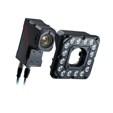
Charge-coupled devices (CCD) and CMOS sensors both convert light into electrical signals. However, they differ in how they transfer and process data. CCD sensors move accumulated charge across the sensor to a single output node, an approach that produces uniform signal characteristics, but it increases demand on power supplies and limits the readout speed of the data. CMOS sensors process data at the pixel level and allow faster readout, and support greater integration of supporting circuitry on the sensor itself. This design promotes compact camera setups and simplifies system integration in many machine vision systems, like the VS Series.
CCD sensors still appear in specialized applications that prioritize uniformity or long exposure performance. In most industrial vision systems, however, CMOS sensors are selected for their balance of speed and efficiency.
Master the basics of vision systems with the KEYENCE today.
Summary of CCD and Image Processing Basics
Machine vision can detect areas (No. of pixels), positions (point of change in intensity), and defects (change in amount of intensity) with 256-level intensity data per pixel of a CCD image sensor. By selecting systems with higher pixel levels can higher speeds, you can easily expand the number of possible applications for your industry.
As image processing needs to detect change of intensity data using calculations, a clear image must be captured in order to ensure stable detection.

Related Downloads

This guide is a compilation of trivia pertaining to vision systems. Figures are used to provide easy-to-understand explanations of principles and characteristics for items ranging from lenses, image capturing, lighting, and color to communication and preprocessing. This guide is a must-read for anyone wanting to learn all about vision systems.

Related Products
Industries
- Aerospace
- Automation Equipment/Machine Building
- Automotive
- Commodities
- Defense
- Electric Vehicles
- Electronic Device
- Fabric/Textile
- Food/Beverage Packaging
- Logistics
- Machine Tools
- Marine
- Medical Device Manufacturing
- Mining/Metals
- Paper Manufacturing
- Pharmaceuticals
- Printing
- Semiconductor/Manufacturing Electronics
- Solar
- Tobacco
- Vision-Guided Robotics
